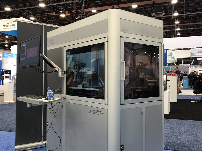
Israeli PCB print leader Nano Dimension showed off its DragonFly 2020 Pro 3D printer at a US event for the first time while attending RAPID + TCT in Texas last year. Not too long ago, I finally had the opportunity to see the machine for myself while attending this year’s RAPID in Detroit, Michigan.
The industrial PCB printer was the first thing I saw at the booth – it’s hard to miss, being much taller than its desktop predecessor. The system stands on the floor and offers a larger footprint, though it has the same 20 x 20 cm print area as the original DragonFly 2020, which officially ended its beta program in the summer of 2017. Tim Sheehan, the VP of Global Sales and Customer Care for Nano Dimension USA Inc., came over to greet me, and we sat down to chat.
 Sheehan used the example of an electrical engineer looking to make a prototype board, noting that everything involved in the process – from finding a business to make the prototype, filling out and getting a purchase order approved, having the prototype made and getting it shipped to you – can cost thousands of dollars and take months to complete.
“That’s the standard process that people deal with today,” he said.
“Now, along comes someone who says, what if I could increase your productivity and reduce your cycle time…that’s giving you a return on investment that’s going to help.”
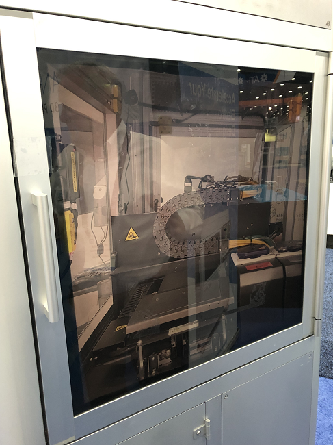
Then we walked over to the DragonFly 2020 Pro so I could get a closer look. Sheehan explained that a dielectric ink (DI) and a conductive ink are both cured at almost the same time within the system.
“It takes sophisticated software to calculate the algorithm to make sure that what you want to be a feature on that board…something as simple as a hole…it places the hole each time at the appropriate place.
“The board is being printed on a chuck, and that chuck is a heating element and a holding element, so it’s holding what’s being printed.”
The chuck moves back and forth, while the ink is being distributed exactly where it’s supposed to go. Nano Dimension uses a free SOLIDWORKS add-in which, according to its website, “creates a design environment optimized for 3D printing multi-material electronics.”
“So all of this can allow that electrical engineer not to take all that time – that two days for approval, a week to get all the signatures, three to five weeks for the board to show back up, ordering of components – all that time. You can now have a board printed overnight.”
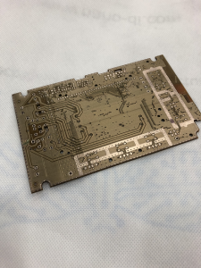
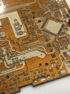
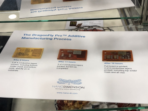
Sheehan told me that, as an engineer, the first design you come up with is never the best. The DragonFly 2020 Pro really helps to speed up the design process, so if you need to make changes and iterations, you’re not wasting everyone’s time. He then showed me some examples of what the PCB printer is capable of, including a 12-layer PCB (below) that took a total of 20 hours to print.
“Time is only determined by the amount of silver we want to put down,” he explained.
“No one else in here can do this. The only way this is being done is the old-fashioned, traditional way, which is one layer at a time is created.”
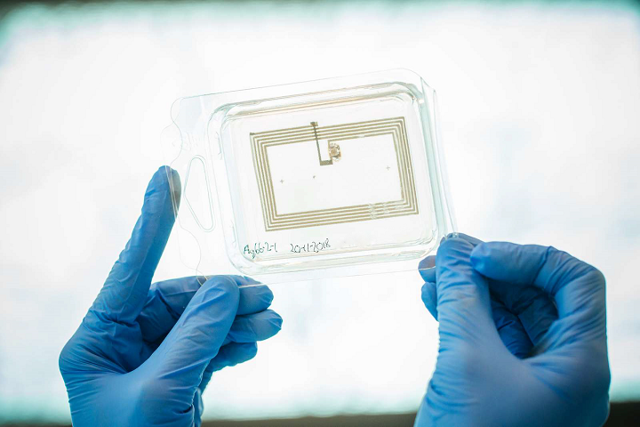
He also showed me a PCB with an indentation on one end where a battery will sit, which also features a circuit that’s on multiple layers.
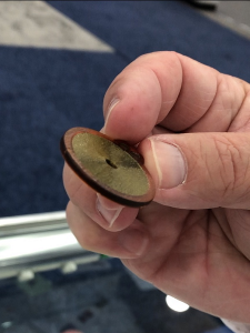
Next, Sheehan brought out a sample that demonstrates a helical conductive coil – created in 180 extremely fine turns – that’s embedded in the company’s dielectric ink; this shows Nano Dimension’s ability to create non-planar conductors, and embed them in a structure, in a single process. This can be used in applications such as charging cell phones or as a solenoid, which acts like a magnet when carrying electric current.
“Solenoids generally grab something locked…unlock the solenoid, door opens,” he explained.
“I have children, I’m not home, they come home from school, the door opens, the signal gets sent, I know they’re home. This is the whole IoT, right? Related to electronics.
“So how this all plays through for us is I’m helping you increase productivity.”
I asked Sheehan if anything new was happening with Nano Dimension that he could tell me about, and he said that the company had recently begun a European expansion, in addition to completing its partner development in North America.
“We’ve signed on national and global leaders in additive manufacturing.”
He listed some of these, including additive solutions and SOLIDWORKS software reseller Go Engineer, CATI, and Fisher Unitech, which is the largest Stratasys reseller in the world.

“So, what else is new for us? A lot of what we call application development sharing – we’re introducing how we can help people side mount components, how we can help people create three-dimensional applications, like the inductive coil,” Sheehan explained. “That’s just a few of the many different, what we call ‘feature applications,’ we’re introducing to help people stretch their minds around what else you can do with the DragonFly.”
Nano Dimension has been listening to its customers, and until this point, the company’s “addressable market” has been R&D with major research institutes. But now, the US Department of Defense is one of the top markets it’s addressing, after becoming a certified DoD vendor last June.
“They are the biggest single organization buying from us today,” Sheehan said, noting that Tier 1 suppliers are also purchasing DragonFly printers. “There are different Army, Navy, Air Force branches buying this system, doing things that we don’t even really know because it’s not for us to know…we’re probably not allowed to know.
“So that’s exciting because when you bring a product to market, you want to know who to address in the market, you want to make sure you go target that. But what’s important is we gather the information from them, and then come back and do the appropriate things for the future of the product. So that’s been successful for us.”
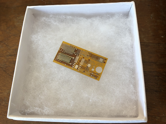
Before I left, Sheehan presented me with my very own 3D PCB, which now sits on my desk next to a myriad of other prints I’ve made or been given. I was excited to receive the PCB, not only because it’s a good physical reminder of what 3D printing is capable of, but also, as I said to Sheehan, who doesn’t like to be handed a little white box?
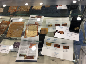
Stay tuned for more on 3DPrint.com’s trip to RAPID + TCT 2019, and take a look at more pictures from the Nano Dimension booth below:
Discuss this story and other 3D printing topics at 3DPrintBoard.com or share your thoughts below.
[Images: Sarah Saunders]

 New Mexico-based Optomec, which supplies production-grade 3D printing systems for electronics applications and LENS Directed Energy Deposition 3D printers for the manufacturing of metal parts and components, just announced that Samsung Electronics will be using its patented Aerosol Jet technology. This week, it was revealed that Samsung has commissioned one of Optomec’s Aerosol Jet (AJ) 5X 3D printers, which will be put to work in its Printed Electronics Lab for the fabrication of next-generation consumer electronics.