At Every Unique Voxel a Unique Design and Material Best Suited for That Point and Application.

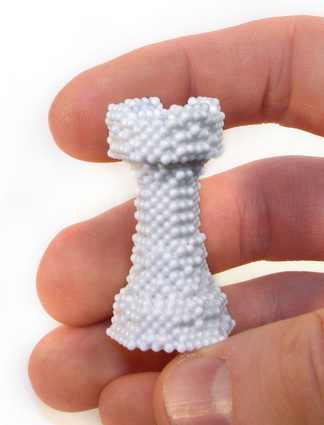
An example of a Voxelfab object by Jon Hiller.

A voxel is a 3D pixel. A unit of 3D dimensional space, a voxel can be a virtually demarcated space in a 3D file or it could be somewhere on a physical object. Voxels can be assigned values relating to the single point that they represent. You could describe a voxel’s density, color, conductivity etc. all as related to that single point that you identify. That one point is then located precisely. Voxel as a concept is easy enough to understand, but it is underutilized in 3D printing at the moment. Voxels let us imagine a world where everything is made up of discrete Lego blocks that we can identify and assign properties to. If we’re thinking of a programmable physical world then this as a concept is very exciting. Instead of the world being a pancake mix where a material might be malleable and changeable when you make it, the world is definable at every single point. Materials are not just a sludge that we pour out, to harden and become things. Materials can be defined not only on aggregate but with individual characteristics at every single location.

If we’re talking about gradient materials where we can change the density of a 3D printed part as well as its flexibility and hardness we can see that as an industry we are already looking at this space. Functionally graded (or gradient) materials are emerging. Stratasys Objet printers are already able to look at the voxel and what characteristics it may have. Envisiontec already looks at how it can harden a particular voxel of a resin bath. As a design idea, its also represented well by all of the pixel art type of stuff that cool folks put out. If we look at the papers of Jon Hiller and Hod Lipson however from years ago then we’re still a bit behind. Papers about 3D printing self-aligning parallel voxel manipulation and tunable material properties for 3D voxel printers are still not commercialized. Their continuation of a concept by Gershenfeld (I’m sure of it but I can’t find it anywhere online) is still fresh to most of us. Their ideas and research into cellular machines go much further still and imagine billions of micron-sized building blocks being assembled into parts.Even though initial voxelfab machines have been created the thinking to continue this in the industry is simply not there. I’ve been enamored with the voxelfab idea for a long time now. Indeed that’s why my consultancy and blog are called Voxelfab. The idea of being able to program, select and assign properties to every little Lego block you used to build something still blow my mind. How idiotic is our current way of building and making things? I take a block that has the characteristics I want and cut out the shape I need. Or I take a material and slather it on a layer by layer. It’s just silly. So imprecise and limiting. There are encouraging signs though that the age of the voxel will emerge. But, rather than making the voxels first, in an efficient lithographic process for example and then assembling them in a “select, assign, scoop, deposit” process to a point in a part it is microstructure control that comes the closest now to looking at the voxel.

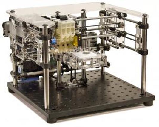
Jon Hiller’s Voxeljet (2008)

The metal 3D printing people have found that by changing the variables of their process they can control individual microstructures which can then give their parts different properties. The melt pool, melt pool velocity, feed rates, temperatures, spot size and all of the variables inside the melt pool are being looked at. Companies such as Digital Alloys talk about being able to determine where each voxel is to determine final part properties. A big trend in papers is in microstructure control of metal printing. Gold nanostrctures are being 3D printed, looking at nano sized structures through the nanoscribe and other machines, we’re looking at how build orientation influences microstructure, seeing colonies of cells in metal prints, EOS’s to be released LaserProFusion technology points a million lasers at discrete points in a build to harden that one point. One could see LaserProFusion being used to create different characteristics of voxels at each point. By taking the pancake batter and pouring power into it the metals people are trying hard to make voxels out of the soup and gloop that our world is made out of.

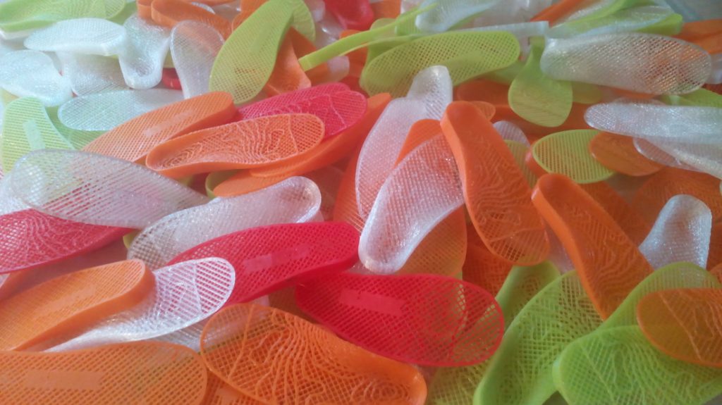
Whilst OEMs and researchers are thinking of this it is designers who are really lagging. Let’s take a great example: Steve Wood’s variable density insoles. In these, we can take unique pressure pad and scan data to vary the infill in an FDM (material extrusion, FFF if you’re a tool) print. This infill itself is a pattern such as a hexagon. This means that in these insoles we’re creating a unique material just for one of your feet and your walking mechanics/issues. This is an exciting and totally doable thing that will in and of itself change footwear forever. But, what if we went a step further still and were able to consider FDM infill, not as a (often randomly chosen) pattern but a true 3D pattern that we can change at every point? What if we vary this pattern and the infill all throughout the build? What if we control the voxel that hardens out of our nozzle as well? Much more directly by cooling or heating it directly? What if in FDM we can at the single point control exactly what we are building? What if in addition to the temperature we can also precisely control for the shape of the voxel being deposited as it is deposited and then also vary the pattern in which it is deposited. Cray cray idea right? But, that would let us do the same. This would let us create a single material at every single point in a print. Every point would be ideally suited to its purpose. Everything would be a unique material best made for what it should be. This explains my obsession with the idea of “crystallization on the fly” in polymers. What if we could go from building an object one layer at a time to building an object one voxel at a time? This would let us completely change how things are made. To me voxelfab is still the complete dream outcome of what we should be able to do and a decade in the darkness I can see outlines of it emerging. At Every Unique Voxel a Unique Design and Material Best Suited for That Point and Application. Will you take up the torch?

Interview With Kevin Eckes of Selective Powder Deposition Firm Aerosint

Most new startups in 3D printing are rather boring. There’s lots of whizzbang but very little fundamental innovation. Most of them are looking to score not looking to improve 3D printing as a whole. Aerosint may very well be one of the few startups that could bring true innovation to 3D printing. The startup is looking to change how powder bed systems recoat themselves, how they deal with supports and in the process open up a whole host of new materials and applications while also reducing the cost of parts. We interviewed Kevin Eckes of Aerosint to find out more about this potentially very exciting startup.

What is Aerosint?

Aerosint is a company founded in 2016 on the idea that selective powder deposition will make additive manufacturing more capable, scalable, and less expensive. We have developed a mechanical system that replaces the normal powder recoater in SLS/SLM systems so that multiple powders can be deposited in a single layer with spatial selectivity.

What challenges do you hope to solve for people?

We believe our technology will allow for the scaled production of advanced parts that are topology-, material-, and cost-optimized. Most powder bed fusion AM techniques currently are focused primarily on geometric capability, far less on part cost, and almost not at all on efficiency gains through the use of multiple materials. In short, we want to help additive manufacturing live up to its hype and be able to build the best parts possible at the lowest cost.

How does your technology work?

The system we have developed deposits small ‘voxels’ of powder in a line-by-line fashion from rotating drums that pass over a build platform in an SLS or SLM machine. Unlike the single-material recoating process used in SLS/SLM/MJF/binder-jetting processes, in using our system one has full three-dimensional control over powder material placement, which is required for building multi-material parts.

Why is the rotating drum essential?

It’s the most efficient geometry for the application. With a rotating drum the only limits of the X and Z dimensions are the size of the machine enclosing the Aerosint recoater system. The length of the rotating drum (i.e. axial dimension) limits the Y-dimension of the build.

What do you mean with multi-material?

We mean, quite literally, more than one material. Our system can pattern two or more powdered materials side by side. Of course, sintering them together is an altogether different matter, and we cannot circumvent fundamental physical limitations. Therefore, two polymers or two metals with similar thermal processing temperatures can realistically be incorporated into a single part using the Aerosint powder deposition system to structure the constituent powders prior to sintering.

There’s also a possibility of making what we call “pseudo multi-material” parts. These would be parts in which the bulk of the part is a base polymer, and certain regions include composite materials composed of the same base polymer with an additive, such as glass fiber, carbon fiber, or even nanoparticles to locally enhance the part’s mechanical, electrical, or magnetic properties.

Recently we’ve demonstrated the co-deposition and sintering of flexible TPU with rigid polystyrene (left) as well as multiple colors of TPU (right).

Can you do gradient materials as well? Gradient and multiple materials at the same time?

You can think of the powder images we create as physical versions of binary (i.e. black and white) images. So, while we can’t pattern truly continuous gradients we can do dithered ‘digital’ gradients to form interfaces between two materials (see above, left). In our system, theoretically, you can pattern as many materials as you have rotating drums. In practice, there is, of course, a limit based on the machine size but 2, 3, or 4 drums per machine could be realized.

How can this be used to optimize surfaces?

Surfaces can be optimized in terms of material properties and material savings. One useful application is to be able to create parts that have a hard surface material to resist wear and abrasion combined with a tough inner material to resist brittle fracture (left). This strategy is even more attractive if the cost of the surface material is high relative to the bulk material. In another example, a copper part with high thermal conductivity can be made stronger and more resistant to stress with a steel surface (right).

What are the advantages of this (relative to other AM techniques)?

The most mature multi-material 3D printing processes are dependent on the curing of multiple expensive polymer resins, sometimes containing nanoparticles (as is the case for conductive resins). These resins are often quite expensive, and they tend to age and become brittle after printing. Because of these and other disadvantages, this resin jetting and curing process is better suited for prototyping rather than production-scale AM.

Powder bed AM processes have proven to be the fastest, most cost-effective, and scalable of all the various AM methods. We wanted to develop a process that builds on existing powder bed technology to make it able to process multiple materials. Our powder deposition system is also material-agnostic — we can handle polymer, ceramic, and many metal powders.

What are the cost advantages of your technology compared to SLS?

SLS of polymers is rather wasteful because unfused powder that has undergone an hours-long heated build process changes chemically in ways that prohibit its direct re-use in a subsequent build. Some amount can be reused when mixed with virgin powder, but there is almost always an amount which is thrown away.

The problem is worse for high sintering temperature materials, such as PEEK and other high-performance thermoplastics. It happens that these materials are also quite expensive to begin with, so any powder savings translates to significant cost savings. Our system allows for the deposition of expensive build powders only where needed, because a cheap, non-fusing support powder (such as ceramic) can be co-deposited in each layer.

By using ceramic powders as reusable support how much money would I save? 

With conservative assumptions for build density and powder refresh rate based on data provided to us by a major service bureau, we estimate that the value of material wasted in a full build of PEEK powder printed in an EOS P800 system is about 32,000 USD. After only 38 full builds, the cost of powder waste would exceed the cost of the EOS P800 machine itself!

For PA12 and similar conservative assumptions, for a full build in an EOS P760 system the powder waste cost amounts to nearly 3,000 USD.

With an Aerosint recoater depositing both non-fusing ceramic support powder and polymer build powder, we believe the powder waste rate could be reduced to less than 1% of the overall amount of powder input in the process. For PEEK this represents less than 500 USD/build, or a savings of over 31,500 USD savings per build. In the case of PA12 the waste would be reduced to 74 USD/build, corresponding to a savings of 2,926 USD/build. Considering the hundreds of builds a major service bureau would do per year per machine, the cumulative savings can easily amount to millions of dollars per year.

A more detailed analysis is here

What materials are you working on?

For the multi-material case, we have active projects to combine flexible and rigid polymers like TPU and PA12, multi-colored polymers, and steel and copper. For the powder savings case we are focused almost exclusively on PEEK, and we’re developing a powder deposition system that will withstand the extreme operating conditions needed for PEEK SLS.

I don’t see how you could use this to combine 3D printing circuits and polymers in one step. Won’t you melt or deform the polymer?

For circuits, indeed an approach cleverer than simply melting copper and polymer side by side is needed since bulk copper has a much higher melting temperature than any thermoplastic. We know of some interesting work being done to develop sinterable polymer composite materials that can be made selectively conductive in a post-processing step. As long as the matrix polymer of the conductive precursor material has a similar melting temperature as the surrounding bulk material, it should be possible to print conductive paths and insulating material at once using our system.

What kind of metals can you combine with each other?

Our first efforts are focused on steel and copper. With the same prototype system other metal-metal combinations should eventually be possible to validate.

How mature is your technology?

Our technology is maturing quickly but many aspects still need to be validated. In particular we need to combine our powder deposition expertise with the materials processing expertise of others to push our technology closer to the market.

What kind of partners are you looking for, and why should they work with you?

Our technology should enable multi-material AM, but we have limited in-house experience and resources to explore the space of material combinations that might be possible. We’re interested in working with research institutions and especially R&D departments of companies that have identified a need for multi-material additive manufacturing for improving their products and market position.

We’ll have a booth next week at Formnext in Frankfurt among the other startup challenge winners, and we welcome anyone to stop by to discuss applications and collaboration possibilities.