
A substantially faster means of producing 3D printed electronics has been devised by a team of researchers from the University of California Los Angeles (UCLA). The new approach is nearly five times quicker than conventional techniques and has the potential to expand the applications of additive manufacturing in consumer electronics such as advanced prosthetics, metamaterials, […]
3D Printing News Briefs: February 21, 2020
In today’s 3D Printing News Briefs, we’re talking about new products and materials, an industry event, 3D printed electronics, and education. 3Doodler announced a new product, and Essentium will be showcasing two new materials at RAPID + TCT. The 4th annual AM Cluster of Ohio conference is coming up in July, and nScrypt is microdispensing 50um dots for 3D printed electronics. Finally, Penn State University is investing in Roboze technology.
3Doodler Introduces New 3D Build & Play
 At the New York Toy Fair, February 22-25 at Manhattan’s Jacob Javits Center, 3Doodler will be showcasing its latest device – the 3D Build & Play, perfect for preschoolers and kindergartners to use. The pen was designed for users as young as four years old, and introduces growing children to 3D printing technology in a way that promotes cognitive and fine motor skills development, hands-on learning, story telling, and three-dimensional thinking. The 3D Build & Play is kid-safe, extruding low-heat, BPA-free, non-toxic, biodegradable plastic, and comes with a story-based Activity Guide so parents and kids can create together. Currently available for pre-order, 3D Build & Play will have an MSRP of $29.99, and major retailers, like Amazon, are also expected to carry the product in Q2 2020. Visit 3Doodler in Booth #2771 at the New York Toy Fair to learn more.
“3D Build & Play brings the creative fun of our Start pen without the learning curve for the youngest users. The system we have developed, that lets kids crank and create in 3D, is a major benefit for parents looking to improve their children’s basic motor skills. The included molds make it easy to create 3D objects by simply filling and popping them out. There’s nothing on the market today that makes 3D creation this simple or fast for young creators,” said 3Doodler’s CEO Daniel Cowen.
Essentium’s New Materials for High-Temperature Applications
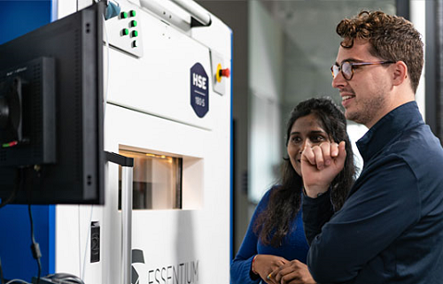 At RAPID + TCT 2020 in Anaheim this spring, 3D printing solutions provider Essentium will introduce new ULTEM AM9085F and ABS materials for high-temperature industrial AM applications. These high-performance materials, which will be showcased on the company’s High Speed Extrusion platform at the event, provide high strength and have excellent resistance to heat and chemicals at high temperatures, so they can be used for applications in the aerospace, automotive, industrial, and medical industries.
According to a survey commissioned by Essentium, 51% of executives believe that the high cost of materials is a major obstacle when it comes to adopting 3D printing for large-scale production purposes. The new ULTEM AM9085F and ABS materials were created to give manufacturers a more cost-effective solution when compared to expensive closed-system materials. Learn more at Essentium’s Booth #3400 at RAPID + TCT in Anaheim, CA, April 20-23, 2020.
4th Annual Additive Manufacturing Cluster of Ohio Conference
 The Additive Manufacturing Cluster of Ohio, powered by organizations such as America Makes and the Youngstown Business Incubator, has announced that its 4th annual conference will take place this summer in Cleveland. Cluster members work together to create a supply chain of interconnected institutions and businesses to advance regional growth in 3D printing. This conference, to be held on Thursday, July 30, at the Embassy Suites by Hilton Cleveland Rockside, will be the first cluster event of 2020, and will give Ohio manufacturers of multiple business models and sizes perspectives on available opportunities for adopting 3D printing into their process chain over the next five years.
The website states, “The program will look at similarities and differences across several selected manufacturer types and will identify strategies ranging from low to high risk. Attendees will leave with actionable strategies and information about regional resources to help them remain competitive in the evolving manufacturing landscape.”
nScrypt Working with 3D Printed Electronics
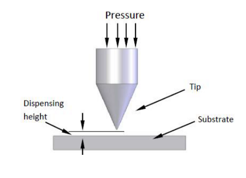 Orlando company nScrypt is working with precision microdispensing, an additive method of dispensing pastes, inks, and other fluid materials, to create adhesive dots with volumetric control, in the 50 micron range, for 3D printed electronics and flexible hybrid electronics (FHE). Microdispensing gets much closer to the substrate surface when compared to methods like jetting, and the closer the nozzle is to the surface, the finer the features of the 3D printed parts. The team used the nScrypt SmartPump, a silicone adhesive, a conical pen tip, and Heraeus SAC305-8XM8-D Type IX solder paste, and tested the consistency and repeatability of ~50µm Type IX solder and adhesive dots.
These tests showed a consistent average dot diameter of 51.24 microns, with a 6.42 micron (13%) standard deviation. These results support the fabrication of 3D printed electronics through the use of direct digital manufacturing (DDM), which allows printing to both planar substrates and the non-planar world of Printed Circuit Structures, which prints the housing or structure of an electronic device as well as placing the electronics conformally. In the future, the team plans to conduct a larger solder and adhesive dot study, in order to test required downtime, long-term reliability, and the frequency of clogging.
Penn State University Invests in Roboze Technology
 Penn State, a 3D printing leader through its Center for Innovative Materials Processing through Direct Digital Deposition (CIMP-3D), has invested in a new FFF solution in order to expand its AM capabilities. The ROBOZE One+400 Xtreme 3D printer, which was designed to create high performing, functional finished parts in advanced composite materials, will help the university increase its development of high performance plastics for 3D printing, and will be housed in the Department of Chemical Engineering. Students will be able to test out new polymers on the system, and develop new formulations to provide 3D printed parts with multi-functionality. These parts will be used to advance research in applications like chemical reactors.
“ROBOZE One+400 Xtreme will be used to examine novel polymers to help to fundamentally understand the 3D printing process and as a tool to enable custom equipment more cost effectively than can be obtained with machining metals while also allowing for designs not possible with traditional manufacture. The ROBOZE One+400 Xtreme will allow Penn State to leverage its expertise in materials science, engineering and characterization to enable new solutions to problems through additive manufacturing,” said Professor Bryan D. Vogt from the Department of Chemical Engineering.
“The ability to use custom filaments and control the print processing was a critical factor in selecting ROBOZE. The flexibility allowed by ROBOZE along with its excellent printing capabilities is well aligned with the discovery-oriented research mission of the university to expand knowledge and its application. Moverover, our prior 3D printer had issues printing high temperature engineering plastics like PEEK with severe deformation of the structure generally observed. After challenges with printing PEEK with standard belt driven systems, the novel direct drive approach with the ROBOZE was an added bonus.”
Discuss these stories and other 3D printing topics at 3DPrintBoard.com or share your thoughts in the Facebook comments below.
The post 3D Printing News Briefs: February 21, 2020 appeared first on 3DPrint.com | The Voice of 3D Printing / Additive Manufacturing.
Robotics Manufacturing at the Next Level with 4D Printed Soft Robotics
Authors Ali Zolfagharian, Akif Kaynak, and Abbas Kouzani explore the growing science of soft robotics, outlining their findings in the recently published ‘Closed-loop 4D-printed soft robots.’ Emphasizing how fast this field is growing, the authors make it clear that many different levels of research and development are involved, from materials and modeling to performance control and more. 3D printing allows for great customization but in taking the process to the next dimension with 4D printing, researchers can add much greater functionality to robotics.
Closed loop 4D printing allows researchers to enhance soft robots with sensors, actuators, and controls for better performance overall. The authors integrated such details into their electronic innovations here, using a data-driven, machine-learning model meant to handle a new hierarchy of tasks to include:
- Grasping
- Sorting
- Climbing or crawling
- Inspecting
- Search and rescue
- Drug delivery systems
“Origami-like soft robots can provide variable stiffness with higher efficiency and dexterity required in specific tasks, which conventional robots cannot handle,” stated the researchers. “Closed-loop 4D-printed soft robots may be also used in autonomous surgeries, laparoscopy, and endoscopy.”
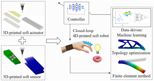
Diagram of closed-loop 4D-printed soft robot.
Machine learning plays an obvious—and substantial—role in 4D printed soft robots, alleviating some of the challenges involved in ‘diverse manipulation tasks.’ Machine learning can be used to develop such robotics during the manufacturing process, and algorithms can be used to speed up property optimization like viscosity and orientation of parts.
“Through the integration of physical models, the ML uses sparse datasets in a statistical learning framework to predict materials and 3D printing processing parameters to increase 3D printing speed and fidelity,” stated the researchers.
With 3D printing, the following features can be introduced:
- Targeted anisotropy
- Variable stiffness
- Spatially heterogeneous mechanical strengths
The use of machine learning is advantageous for this area of robotics, offering increased dimension and more, with a variety of control mechanisms available: open-loop controllers, closed-loop (with embedded soft sensors), and more.
“The mechanisms and materials used in the construction of soft robots are similar; hence, the control can be inspired by a learning strategy that deals with high nonlinearity and agility,” explain the researchers.
3D-printed sensors with applications in 4D-printed soft robots. (a) 3D-printed integrated strain sensor (reproduced with permission from Copernicus Publications on behalf of AMA [42]); (b) 3D-printed sEMG electrodes (reproduced with permission from Copernicus Publications on behalf of AMA [42]); (c) 3D-printed piezoelectric sensor in jellyfish soft robot (reproduced with permission from SPIE [67]); (d) 3D-printed e-tongue sensor (reproduced with permission from Frontiers [110]); (e) 3D-printed pressure sensors (reproduced with permission from John Willey and Sons [71]); (f) 3D-printed fluid flow rate sensor (reproduced with permission from IOP Publishing [98]). (g) 3D-printed dog nose for gas detection (reproduced with permission from Nature Publishing Group [109]); (h) 3D-printed flexible tactile sensor (reproduced with permission from Springer [58]); (i) 3D-printed thermochromic and solvatochromic sensors (reproduced with permission from John Wiley and Sons [100]).
Just 3D printed sensors alone are now advanced enough to be printed in spatial levels, and with 4D printed robotics, such features can be ‘categorized and introduced.’ There is also the possibility for the potential of amphibian soft robots able to perform a wide range of tasks.
“Despite existing problems, 4D-printed soft robots are achievable through the integration of 3D-printed soft sensors and actuators with machine learning algorithms and FEM,” concluded the researchers. “Integrated 3D-printed actuators and sensors are feasible but limited by the nature of materials utilized. The future of enhancing closed-loop 4D-printed soft robots accordingly relies on integration of suitable materials, machine learning approaches and control algorithms.”
Soft robotics continue to be increased subject of research, from new designs and frameworks to continued customizations and different materials. What do you think of this news? Let us know your thoughts; join the discussion of this and other 3D printing topics at 3DPrintBoard.com.
Integrated 3D-printed soft sensors and actuators: (a) 3D-printed embedded sensor in pneumatic soft actuator (reproduced with permission from SPIE [126]); (b) 3D-printed soft gripper with printed embedded sensors (reproduced with permission from John Wiley and Sons [9]); (c) 3D-printed tactile sensor on 3D-printed prosthetic hand (reproduced with permission from the American Chemical Society [34]); (d) 4D-printed multistable thermal actuator (reproduced with permission from John Wiley and Sons [150]); (e) Bistable 3D-printed soft actuator (reproduced with permission from MDPI [148]); (f) 3D-printed variable stiffness soft actuator with an integrated joule heating circuit (reproduced with permission from John Wiley and Sons [151]).
[Source / Images: ‘Closed-loop 4D-printed soft robots’]
The post Robotics Manufacturing at the Next Level with 4D Printed Soft Robotics appeared first on 3DPrint.com | The Voice of 3D Printing / Additive Manufacturing.
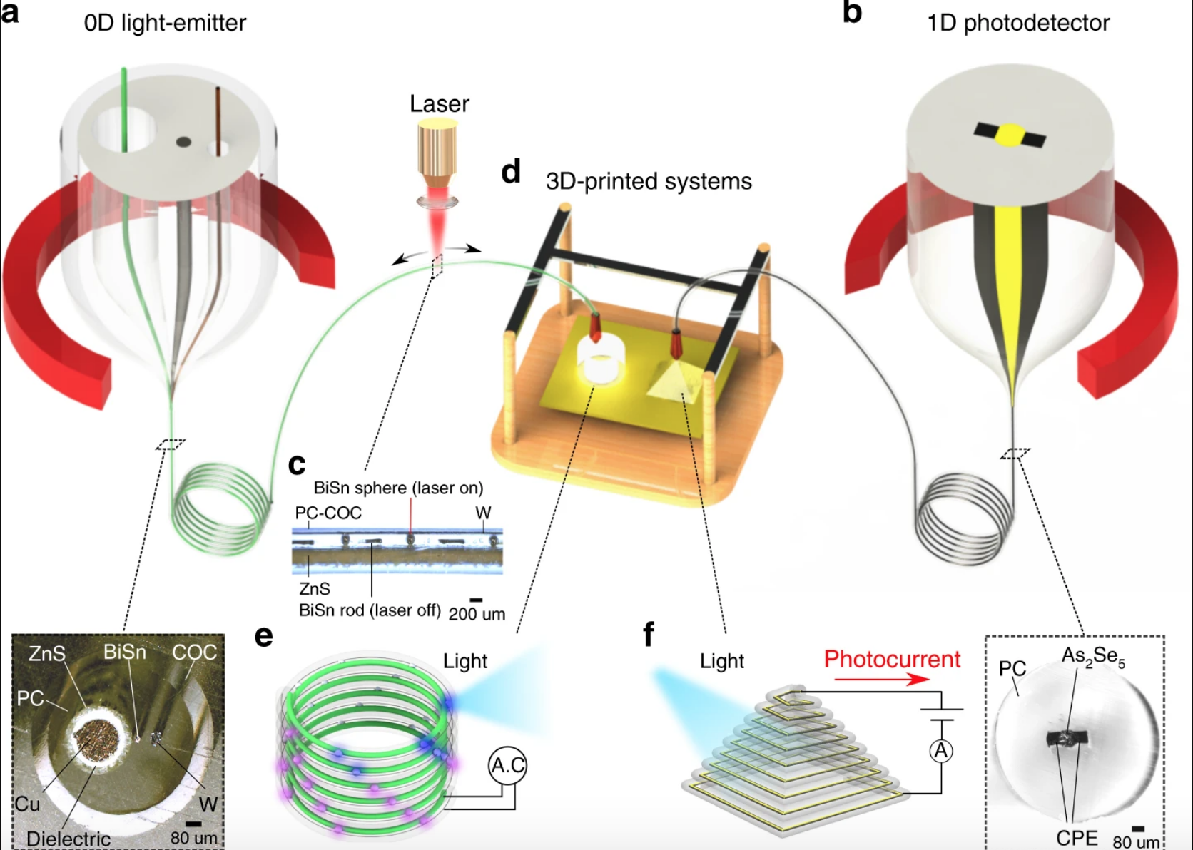
MIT: A New Fiber Ink With Electronics Embedded Inside
Innovations in printed electronic devices have led to the development of alternative approaches and exciting  applications for 3D printing, focusing on both printing methods and ink materials. It is a growing and evolving field which promises lower costs as well as opportunities for innovative functionality which tends to be more expensive with conventional electronics. Just imagine being able to 3D print an entire model airplane wing, using filaments that contain both light emitters and light detectors embedded in the material, so that it could continuously detect any microscopic cracks as they begin to form.
This is what MIT researchers have been working on, developing a new method that uses standard 3D printers to produce functioning devices with the electronics already embedded inside. The devices are made of fibers containing multiple interconnected materials, which can light up, sense their surroundings, store energy, and more.
According to the new 3D printing method described in a paper by MIT research assistant Gabriel Loke, professors John Joannopoulos, Yoel Fink, Rodger Yuan, Michael Rein, Tural Khudiyev and Yash Jain, the design and fabrication of functional systems shaped in 3D form factors can enable applications in diverse areas such as photonics, sensing, energy storage, and electronics. However, printing different material classes to create electronic devices was, up to now, a complex fabrication challenge in itself, because different print methods were developed specifically for various material classes. The researchers’ alternative approach claims to surpass some of these traditional hurdles.

Gabriel Loke from MIT
“While the filaments used in the model (airplane) wing contained eight different materials, in principle, they could contain even more. Until this work, a printer capable of depositing metals, semiconductors, and polymers in a single platform still did not exist, because printing each of these materials requires different hardware and techniques,” said Loke.
The system makes use of conventional 3D printers outfitted with a special nozzle and a new kind of filament to replace the usual single-material polymer filament, which typically gets fully melted before it’s extruded from the printer’s nozzle. The researchers’ new filament has a complex internal structure made up of different materials arranged in a precise configuration and is surrounded by polymer cladding on the outside.
According to MIT, in the newly reformated printer, the nozzle operates at a lower temperature and pulls the filament through faster than conventional printers do so that only its outer layer gets partially molten. The interior stays cool and solid, with its embedded electronic functions unaffected. In this way, the surface is melted just enough to make it adhere solidly to adjacent filaments during the printing process, to produce a sturdy 3D structure.
The printer used by the team was a RoVa3D multi-nozzle printer, a standard type of 3D printer known as a fused deposition modeling (FDM, material extrusion) printer, which can already be found in many labs, offices, and even homes. While the software used to generate and read the g-code for printing were Slic3r and Prometheus. The hot end was made up of a stainless steel tube that can range up to 2 mm in length and is heated by nichrome wire. Then high-temperature insulation tape is inserted between the hot end and the region above the hot end.
Loke suggested that “this method is up to three times faster than any other current approach to fabricating 3D devices, and as with all 3D printers, it offers much more flexibility regarding the kinds of forms that can be produced than typical manufacturing methods do. Unique to 3D printing, this approach is able to construct devices of any freeform shapes, which are not achievable by any other methods thus far.”
Just a few days ago, MIT’s Computer Science and Artificial Intelligence Laboratory team revealed another ink for use in their 3D printing endeavors, a reprogrammable ink that changes colors upon exposure to UV and other light sources. Known as the PhotoChromeleon system, it is made up of numerous dyes sprayed onto an object’s surface, allowing it to change color as needed. MIT is certainly progressing quickly with functionally engineered creations that keep advancing 3D printing technology even further.
Filaments with embedded circuitry show a lot of promise, they can be used to print complex shapes for biomedical and robotic devices, since the method uses thermally drawn fibers that contain a variety of different materials embedded within them. It is a process that co-author Fink, who is a professor of materials science at MIT as well as of electrical engineering and computer science, along with his collaborators have been perfecting for two decades.
Designable structured multimaterial filament inks for three-dimensional printed functional systems
The internal components of the filament include metal wires that serve as conductors; semiconductors that can be used to control active functions, and polymer insulators to prevent wires from contacting each other.
They have created an array of fibers that have electronic components within them, making the fibers able to carry out a variety of functions. For example, for communications applications, flashing lights can transmit data that is then picked up by other fibers containing light sensors. This approach has for the first time produced fibers, and fabrics woven from them, that have these functions built-in.
Now, this new process makes this whole family of fibers available as the raw material for producing functional 3D devices that can sense, communicate, or store energy.
According to MIT, to make the fibers themselves, the different materials are initially assembled into a larger-scale version called a preform, which is then heated and drawn in a furnace to produce a very narrow fiber that contains all those materials, in their same exact relative positions but greatly reduced in size.
The authors of the research paper claim that in this work, they established a fast, multiscale approach to print a diverse set of designable multi-material filament-based inks to create complex 3D hierarchical functional systems that bridge micron-scale device resolution to centimeter-scale object size. In particular, unlike current composite inks, which have limited control over spatial localization of constituent materials, they assure to have demonstrated structured filaments that combine different interchangeable material classes with controlled interfaces while internal materials can be microstructurally shaped into different topologies to enable varying ink functionalities.
To illustrate the utility of their capability to form complex freeform 3D devices, the researchers combined the 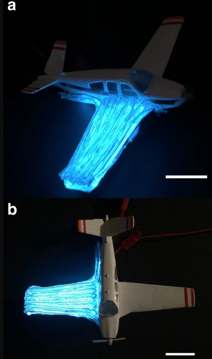 functionalities of both light-emitting and light-detecting within a single printed structure by printing them into an airplane wing, and capable of detecting a structural defect at any point within the wing. The printed airplane wing is seen to have light-emitters at the top and bottom layers, and, light-detectors in the bulk of the wing. As the light-emitters are operated, the photodetectors generate a photocurrent, with its magnitude corresponding to the length of the printed photodetectors filament. Upon the occurrence of a structural defect to the printed structure, the length is cut short, reducing the photocurrent. They can then detect the localized position of damage within the structure. In the paper, the authors describe how this capability is highly applicable for objects that are prone to collisions and high mechanical stresses such as 3D printed drones, prosthetics and parts of mobile vehicles, in which the lack of ability to uncover internal structural defects can lead to major failures.
Moreover, one of the main advantages of the approach is the printing speed, which for this model structure wing took just 24 minutes, much faster than other 3D device fabrication methods. Also, the innovative team noted that the fabrication of such a highly-complex device wing shape can only be achieved through their volumetric freeform device-print approach because it allows for full shape customizability.
This ability to precisely customize each device is essential, and the method could potentially be developed further to produce a variety of different kinds of devices. Including biomedical, where matching the device to the patient’s own body can be important; such as in prosthetic limbs, using all the electronics to monitor and control the limb embedded in place. Additionally, this method might be a perfect fit to print materials for biomedical implants that would provide a scaffolding for the growth of new cells to replace a damaged organ, and include within it sensors to monitor the progress of that growth.
Yoel Fink from MIT
Over the years, the group has developed a wide array of fibers containing different materials and functionalities. Inspired by cucumber plants which use their tightly-coiled tendrils to pull the plants upwards, MIT researchers, including Fink, recently developed a new fiber-based system that could be used as artificial muscles for robots, prosthetic limbs, or other mechanical and biomedical applications. And just last year, they created a type of soft hardware that you can wear, that is, a cloth that has electronic devices built right into it. Fink even went on to create a smart thread that can send messages and change color.
MIT researchers’ idea to 3D print the multimaterial fiber ink in a printed model airplane wing was beyond original. When it comes to the aerospace field, a creation like this could make a big difference.
[Images: Felice Frankel and MIT]
The post MIT: A New Fiber Ink With Electronics Embedded Inside appeared first on 3DPrint.com | The Voice of 3D Printing / Additive Manufacturing.
Electronic Alchemy develops multi-material electronics 3D printer for NASA
3D printer manufacturer Electronic Alchemy has developed a system capable of additive manufacturing fully functional electronics. Named eForge, NASA intends to use the system during planetary space missions to 3D print chemical sensors on demand. Following the launch of eForge, the company is also now designing a device to recycle 3D printed electronics, further reducing […]
Nanyang Technological University: Inkjet Printing of ZnO Micro-Sized Thin Films
![]() In ‘Inkjet-printed ZnO thin film semiconductor for additive manufacturing of electronic devices,’ thesis student Van Thai Tran, from Nanyang Technological University, delves into the realm of fabricating products with conductive materials. As inkjet printing continues to gain popularity for researchers and manufacturers, it is the vehicle for creating a wide variety of innovations, to include tissue engineering and more. Here, however, Tran develops and examines ZnO thin film to promote electrical qualities in hopes of expanding 3D printing processes further overall.
In ‘Inkjet-printed ZnO thin film semiconductor for additive manufacturing of electronic devices,’ thesis student Van Thai Tran, from Nanyang Technological University, delves into the realm of fabricating products with conductive materials. As inkjet printing continues to gain popularity for researchers and manufacturers, it is the vehicle for creating a wide variety of innovations, to include tissue engineering and more. Here, however, Tran develops and examines ZnO thin film to promote electrical qualities in hopes of expanding 3D printing processes further overall.
The author understands the many benefits of 3D printing, as they have unfolded since the mid-80s. Today, the technology has progressed far beyond rapid prototyping, and a wide range of functional products are being made.
“It is expected that 3D printing will play a significant role in the fabrication of goods soon. As a result, the demand for printed functional devices has been raised to fulfill the need for printed consumable products, which are composed of multi-materials,” states Tran. “Hereby, the printed functional devices are not only basic electrical elements, such as resistors, capacitors, and transistors, but also advanced electric devices, such as sensor, solar cells and batteries.
“The construction of a product using 3D printing requires a combination of structural material and functional material. To accomplish the fully additive manufacturing process, printing of functional materials, such as conductor and semiconductor, is crucial.”
ZnO is helpful today in applications like:
- Optoelectronics
- Electronics
- Sensors
- Piezoelectric devices
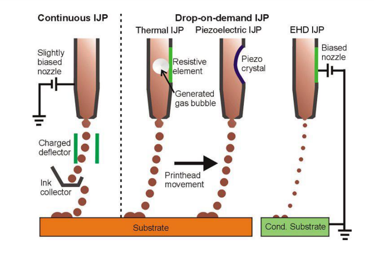
Inkjet printing technologies: Continuous inkjet printing and Drop-on-demand Inkjet printing and electrohydrodynamic inkjet printing
Tran does raise concerns, however, regarding the use of ZnO in inkjet printing—such as the likelihood that it may cause band bending, resulting in defects in the 3D printed products. Band bending issues must be controlled and ‘engineered’ to create a device that is highly functional, lending central focus to this study, along with creating a successful way to improve on using the photolithography process, and investigating issues in annealing.
As an intrinsic n-type semiconductor, ZnO also possesses piezoelectric properties, capable of generating voltage under pressure—and causing it to be suitable for applications requiring sensors and actuators. As for thin film transistors, ZnO is an attractive option due to compatibilities with LCD applications and a variety of miniaturized electronics. As Tran mentions, ZnO is also especially suited to UV photodetector applications too.
In this project, Tran fabricated thin films via inket printing, but modifications were made with annealing—decreasing the band bending. The author also discovered that electrical properties were greatly improved due to heat treatment, with film conductivity impacted by band bending changes.
“The successful inkjet printing of micro-sized ZnO thin films and the integrated photodetector has demonstrated the feasibility and great potentials of fabricating sophisticated semiconductor devices using additive manufacturing technology,” concluded the author.
3D printing and electronics have been coupled together since the beginning, allowing for expansive innovations—and allowing many manufacturers to create items never possible. They are also able to enjoy much greater sustainability in production, whether in creating breakthrough techniques in manufacturing, liquid materials for electronic applications, or wearables. Find out more about semiconductors in AM manufacturing here.
Discuss this article and other 3D printing topics at 3DPrintBoard.com.
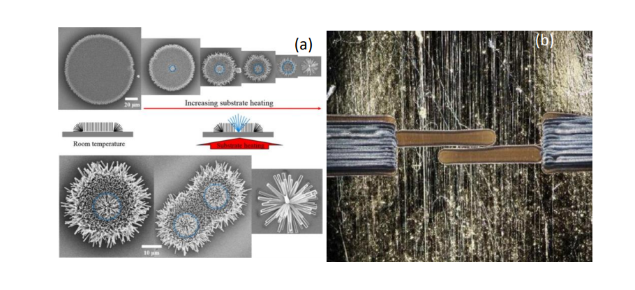
Additively fabricated ZnO nanostructures. (a) Selectively grown ZnO nanowire from inkjet-printed pattern (b) Electro-spinning ZnO nanowire

Printer structure and printing process to prepare the thin film. (a) Printer structure shows the main components and three-axes of the printer. (b) Optical photo of the printer. (c) Optical picture of the cartridge, including ink container and nozzles. (d) The schematic of the droplet watcher, which is the system to observe the generation of droplet before running the printing
[Source / Images: Inkjet-printed ZnO thin film semiconductor for additive manufacturing of electronic devices]
Embedded 3D Printing and Sensors Lead to Soft Robotic Fingers
Robotics and 3D printing have gone hand in hand for years, but researchers Ryan L. Truby, Robert K. Katzschmann, Jennifer A. Lewis, and Daniela Rus have put a much more literal touch on that in their study, ‘Soft Robotic Fingers with Embedded Ionogel Sensors and Discrete Actuation Modes for Somatosensitive Manipulation,’ outlining their latest innovations: grippers that are highly functional due to their adaptability for gripping.
Examples of manipulator poses. Photographs of the soft gripper during no (left), base-only (center), and full-finger actuation at inflation pressures of 140 kPa. Scale bar is 15 mm.
Rigid robots are obviously unwieldy for many applications. Up until now, however, it has still been difficult to design and manufacture soft actuators with the desired features, as they require extensive dexterity in action and a closed-loop control mechanism. Here, 3D printed embedding is the key to making soft robotic grippers shaped like hands, able to show us the future for such devices in applications like:
- Automated assembly
- Packaging
- Prosthetics
- Conservation
- Extreme environments

Examples of object grasping. (a-b) Examples of grasping poses are shown for holding a toy strawberry (a) and pear (b) during base-only (left) and full-finger actuation (right). (c) Examples of objects that can be grasped by the soft gripper with appropriate pre-grasp orientation. Inflation pressure is 140 kPa in each photograph. Scale bars are 15 mm.
“However, creating soft robots with multi-degree-of-freedom (DOF) actuation and somatosensory capabilities remains a significant hurdle that limits their practical use in these areas,” state the researchers. “Most soft robotic manipulators operate via open-loop control and have simple, single-DOF actuation, such as uniform bending or twisting.”
“Given the simplicity of fluidic actuation and molding-based fabrication techniques, fluidic elastomer actuators (FEAs) are a popular platform for producing soft manipulators. Unfortunately, these techniques require multiple assembly steps, especially when multi-DOF actuators are desired.”
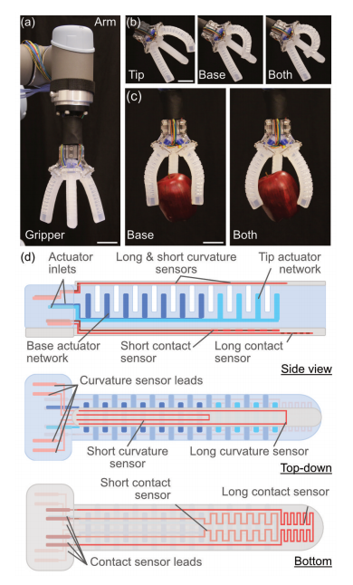
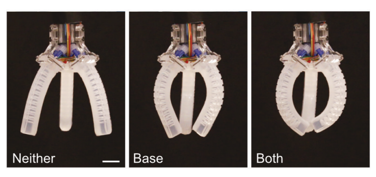
Soft robotic gripper with EMB3D printed soft fingers. (a) Three
fingers comprise a soft gripper fixed to a robot arm. (b) Inflating the tip (left), base (center), or tip and base (right) actuator networks enable three modes of finger bending and (c) different grasps. (d) Schematics of the finger from side (top), top-down (middle), and bottom-up (bottom) views. Scale bars are 30 mm.
The need for sensors often makes devices like this unlikely as greater complexity is added to the design and the actual manufacturing. For this study, and the integration of soft somatosensitive manipulation, the research team strategized on how to make actuators comprised of both discrete actuation modes and integrated sensors. Luckily, they were able to turn to 3D printing, a technology often quite appealing to persistent innovators who know ‘where there is a will there is a way.’
Each finger is made up of two ‘fluidic networks’ running throughout the artificial tip, base, and ‘full-finger actuation.’ There are a variety of different ways that the hand can grip, with four different sensors controlling each digit that contains an organic ionogel for sensory feedback.
“Fabricating FEA-based soft robots with integrated sensors and multi-DOF actuation requires many steps,” state the researchers. “Prior work has used molding techniques to make soft quadrupeds, swimming fish, tentacle-like actuators, and hand-like manipulators with several DOF.”
“By contrast, 3D printing offers a promising approach for rapidly designing and fabricating complex soft actuators. Several light and ink-based printing techniques have recently emerged for directly building multi-DOF soft fingers, legs, grippers, and integrated robotic systems.”
The FEAs may work in either a rigid or soft capacity, but the researchers point out that more traditional, less flexible sensors do not work with FEA soft elastomers. The rigid parts that are required for the elastomeric waveguides do not interface well either. The team goes on to point out also that liquid metal sensors are not a good choice due to the ‘potential displacement of their passivating oxide layers over time.’
As is so often the case in human creativity, science, and 3D design, nature is an enormous inspiration. For this study, the researchers drew on the natural sensory capabilities and dexterity of human hands, creating the three-fingered robotic gripper. Each one was 3D printed using EMB3D printing, which allows for arbitrary patterns to be created—and here, the design is modular. 3D printing took around 90 minutes, curing overnight, and then the parts were refrigerated for an hour to liquefy the ink. The soft fingers were wired together, and then inflated with a pneumatic valve.
“We are now actively pursuing new multi-DOF, sensorized soft actuator designs using these methods to create more complex types of dexterous, soft robotic manipulators,” concluded the researchers. “Soft manipulator designs that we are exploring have different finger numbers, orientations, designs, and sensing motifs than the gripper presented here. Working with established algorithms in grasp planning with soft grippers and object recognition, we aim to develop soft robots with advanced manipulation capabilities that will be useful in myriad applications.”
3D printing allows users (and researchers especially) much more latitude in the lab, and along with accompanying electronics and robotics applications, this often involves experimentation and innovation resulting in items like stretchable electronics, liquid applications, and integration within the internet of things. Find out more about the use of embedded 3D printing for robotics here. What do you think of this news? Let us know your thoughts! Join the discussion of this and other 3D printing topics at 3DPrintBoard.com.
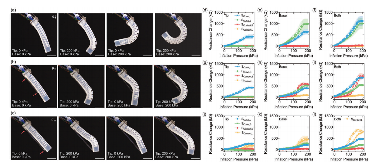
Free and blocked displacement characterization of soft sensorized fingers. (a-c) Photographs of a soft finger in non-inflated (left) and various maximum inflation states for tip (center-left), base (center-right), and full (right) actuation modes during (a) free displacement and blocked displacement with the (b) short and (c) long mounts, whose edges are indicated by the red arrows. Scale bars represent 25 mm; g indicates acceleration due to gravity. (d-l) Resistance change, ∆RS, versus inflation pressure is provided during inflation-deflation cycles (indicated by filled/open circles, respectively) for
the long (SCurve,L) and short curvature (SCurve,S) and short (SContact,S) and long contact (SContact,L) sensors during (d-f) free displacement and blocked displacement with the (g-i) short and (j-l) long mounts. Plots correspond to ∆RS during (d, g, j) tip, (e, h, k) base, and (f, i, l) full-finger actuation. In (l), ∆RS for SContact,L is scaled by a factor of 0.2 (to idenically scale axes across subfigures). (n = 3, error envelopes represent standard deviation.)
[Source / Images: ‘Soft Robotic Fingers with Embedded Ionogel Sensors and Discrete Actuation Modes for Somatosensitive Manipulation’]
European Innovation Hub and Test Bed to Focus on Developing and Implementing 3D Printed Electronics
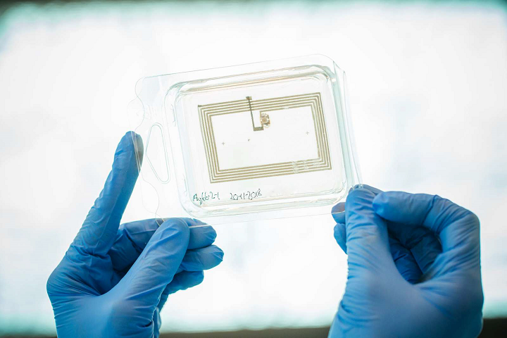
More and more, we are using special industrial 3D printers, with inkjet and aerosol jet technology, to embed conductive components within our intelligent products in what we call 3D printed electronics. Items like ECG electrodes and contactless payment cards use these embedded components to perform wireless activities and readings, like measuring the frequency of a person’s heart beats and paying for something at the store. The technology makes it possible to 3D print conductive circuits on nearly any surface imaginable, and the market for it is estimated at $32 billion outside Europe alone. Now, the continent is working to play catch-up.
In a move to increase Europe’s competitiveness in this field, and further prepare for Industry 4.0, the European Union’s Horizon 2020 has granted €10.6 million in funding to a new European innovation hub, led by the Danish Technological Institute (DTI), that will focus on 3D printed electronics.
“Printed electronics opens up a whole world of new opportunities, as complex constructions can be embedded just like using 3D printing, at prices able to compete with mass-produced goods,” said Zachary James Davis, DTI’s Project Coordinator for the hub. “Quite simply because electronics can be produced from CAD drawings and printed on flexible materials, as already used in architecture and 3D print.”

DTI researchers have been working with 3D printed electronics since 2016. This work, coupled with its efforts in encouraging the adoption of 3D printing, is what makes the university the perfect leader for the new hub as it works to help Europe’s manufacturing industry gain a strong position. Together with 16 RTOs and businesses, such as Fraunhofer, Eindhoven University of Technology, RISE, and Axia, DTI will develop an open innovation test bed, or LEE-BED, which will function as the hub and focus on 3D printed electronics.

Enterprises that apply to join LEE-BED will have their businesses cases evaluated first. If they are selected to participate, they will receive access to RTOs which most closely match their personal requirements. In addition, the chosen enterprises will also have access to expertise and equipment from designated RTOs in order to support their own 3D printing electronics development efforts, with no financial risk, all the way from the prototyping phase up to pilot production and full-scale manufacturing.
Davis explained, “All the partners in LEE BED will provide their various skills and facilities within printed electronics to enterprises that want to integrate and embed electronics into their products.
“Enterprises will be able to prove the viability of new technologies without major investment and financial risk during the all-important initial phase. We have already started working with jewellery giant Swarovski, looking into the idea of intelligent light in their crystals that can be integrated with clothing and home interiors.”

In addition to Swarovski, LEE-BED also has three other industrial cases with European companies: Acciona, Grafietic, and Maier.

LEE-BED is made up of three phases:
- Technological & economic modeling, including lifecycle analysis, patent research and safety/legislation audit
- The pilot project using current, and upgraded, pilot lines for nanomaterials, nano-enabled formulations, and 2D/3D printing of components
- Knowledge transfer, to include evaluation of intellectual property rights (IPR) and patents, investment possibilities, and standards/safety screening
The purpose of LEE-BED is to spread awareness about 3D printed electronics, and develop and implement them across Europe in order to “break down barriers” for the technology to be used. The goal is to keep the European manufacturing industry in the EU, as opposed to outsourcing high-tech projects elsewhere.
Discuss this and other 3D printing topics at 3DPrintBoard.com or share your thoughts in the Facebook comments below.
[Images provided by Danish Technological Institute]
University of California Researchers Explore Acoustophoresis in Regulating Electrical Composites for 3D Printing
![]() Scientists from University of California Santa Barbara have been exploring the use of acoustophoresis in regulating electrical composites in accompaniment with 3D printing in ‘Flexible Composites with Programmed Electrical Anisotropy Using Acoustophoresis.’ This work expands on the current demand in the marketplace for multifunctional 3D printing materials.
Scientists from University of California Santa Barbara have been exploring the use of acoustophoresis in regulating electrical composites in accompaniment with 3D printing in ‘Flexible Composites with Programmed Electrical Anisotropy Using Acoustophoresis.’ This work expands on the current demand in the marketplace for multifunctional 3D printing materials.
Today we see many different types of conductive materials in 3D printing, but as the researchers point out, there are obstacles due to expense and post-processing that consumes too much time. Their goal is to be able to create functional materials that will further applications in robotics, wearables, and thermal management devices.
The scientists delve into the potential of polymer matrix composites, as they offer the suitable levels of stiffness and both electrical and thermal conductivity. Embedded electrical interconnects show great promise, not only in affordability but also time spent in wiring. Field-assisted assembly may be the best route for creating filler particle assemblies before curing in 3D printing. The research team points out that this method allows them to avoid filler particle size limitations, along with:
- Resolution limitations
- Compatibility issues with materials
- Prohibitive complexity
- Prohibitive cost
- High production time
Acoustic focusing is an assembly technique using pressure to control and rotate particles in a given field. While it has most recently been used in applications like cell sorting, acoustic focusing can be used in direct ink writing as well as stereolithography for integrating various particle structures into parts that are 3D printed. The team of researchers developed a new way to 3D print with electrical circuits in this study, showing that electrical composites can alternate between conductive and insulating, as well as between isotropic and anisotropic.
“In addition, composites patterned with acoustic focusing require an order of magnitude lower particle concentration to reach the same conductivity of conventional dispersed-fiber composites, which here exceeds 5000 S/m. Finally, we demonstrate that these patterned composites can be used as durable flexible conductors, with constant conductivity over 500 cycles to 0.7 mm bending radius,” said the researchers.
This method relies on pressure fields for controlling particles suspended in 3D printing materials, activated with a piezoelectric actuator. The scientists use a two-component system, made up of carbon fibers or silver-coated glass fibers. Composites were cured but without the presence of acoustic focusing, and with all fibers dispersed.
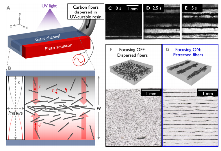
: A Schematic of acoustic focusing device. B Diagram of forces aligning and pushing fibers to the center of a channel as the result of a standing pressure half-wave. C,D,E Time-lapse of fibers patterned into parallel bundles by acoustic focusing in photopolymer resin, reaching equilibrium positions after 5-6 seconds. F Illustration and micrograph of an unpatterned composite with carbon fibers dispersed in acrylate resin (0.36v% carbon fiber). G Illustration and micrograph of a patterned carbon-fiber in acrylate composite (0.36v% carbon fiber) fabricated with acoustic focusing
“The unfocused composites are insulating at fiber volume fractions φ below 3.3%, resulting in an open-circuit measurement. Above 3.3%, these composites have low conductivity (< 1 S/m), with around 1% of the fibers contributing to the conductive network. This transition from insulating to conductive behavior at φ = 3.3% is termed the percolation threshold φc, given by φc = 1/(π/2a + 2a + 3 + π) = 3.3%, where a = l/d is the aspect ratio of the fibers,” stated the researchers.
Fibers are manipulated into bundles via acoustophoresis before UV curing, with spacing of a half-wavelength of the pressure field.
“With acoustic focusing turned on, the conductivity of the patterned carbon-fiber composites is dramatically higher than the unpatterned composites,” state the researchers. “Below the percolation threshold, where the unpatterned composites are insulating, the composites made with acoustic focusing have high conductivity, with up to 98% of the fibers (by volume) contributing to the conductive network.”
The researchers point out that the conductivity found in the patterned composites is ‘invariant from 1-10 percent,’ and the critical volume friction does not rely on fiber length.
“This tolerance to fiber length and loading changes suggests freedom to orthogonally control other material properties, like stiffness, strength, or thermal conductivity, while maintaining high conductivity,” state the researchers.
They go on to demonstrate how electrical transport anisotropy is manipulated in patterned composites, with conductivity parallel to carbon fibers. The scientists point out that as they modulated bundle spacing, they were able to control bridging behavior, then resulting in control of transport pathway density. Such control of line spacing means that electrical conductivity can be modulated for either anisotropic or isotropic properties, allowed ‘on-the-fly’ in 3D printing.
“This versatile technology could pave the way for printing soft components with integrated electrical interconnects, possibly in addition to other integrated functionalities since the conditions for conductivity are lenient,” conclude the researchers. “Acoustic focusing’s material agnostic nature encourages extension to other applications as well, such as thermal management materials, mass/ion transport materials, electroactive materials, and many others.
Acoustics and 3D printing have accompanied each other before in the technological process from soundwave jewelry to acoustic metamaterials and sound data, and engineers and scientists around the world continue to surprise us with innovative combinations. Find out more about the use of acoustics in programmed electrical anisotropy here.
What do you think of this news? Let us know your thoughts! Join the discussion of this and other 3D printing topics at 3DPrintBoard.com.
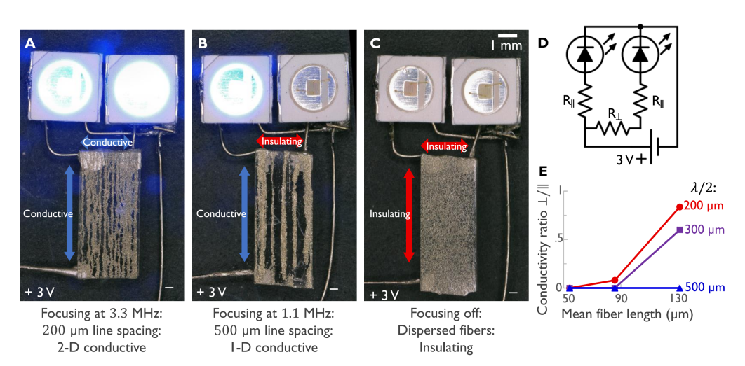
Three composites made using the same precursor ink: A An isotropic conductive 2.6% silver-coated glass fiber composite with focused bundle spacing ∼ 200 µm completing a 3 V circuit to illuminate two 100 mA LEDs. Differences in LED brightness are due to tilt of the metallic reflector with respect to the camera. B An anisotropic conductive 2.6% silver-coated fiber composite with bundle spacing
∼ 600 µm completing a 3 V circuit to illuminate only one 100 mA LEDs. C An insulating 2.6% silver-coated glass fiber composite made with acoustic focusing turned off. D Schematic of the circuit in A-C. E Transport anisotropy in 2.6% composites, given as the ratio of conductivity measured in the direction perpendicular to the focused lines to the that measured parallel.
[Source / Images: ‘Flexible Composites with Programmed Electrical Anisotropy Using Acoustophoresis’]
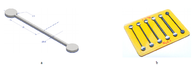
Researchers 3D Print Resistors From Electrically Conductive Filament on a Desktop 3D Printer
In a paper entitled “Characterization of resistors created by fused filament fabrication using electrically-conductive filament,” a pair of researchers 3D prints resistors using electrically conductive carbon black and graphene-based filament.
“With this novel capability to directly create electrical components integrated into 3D printed physical objects designers can envision and 3D print new and/or improved devices with embedded electronics, which they could not do before,” the researchers explain.
Using biodegradable conductive filament to 3D print circuits offers environmental benefits, and 3D printing technology allows for more design freedom, enabling manufacturers to better integrate electrical components within objects. The researchers used a MakerBot Replicator 2X Experimental 3D printer, which has dual extruders, for their work. A test print was created, and then two modifications were made to the 3D printer: an extruder block upgrade, which helped improve the consistency of prints due to reduced slippage of the stepper motor pinion gear; and the attachment of two additional cooling fans, one for each extruder.
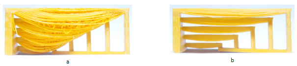
Test piece before (a) and after (b) the modifications
The researchers then designed a cube-shaped resistor using Autodesk Inventor CAD software. Two electrode contact pads were placed at each end.
“To integrate 3D printed circuits with external components such as LEDs, a suitable contact point has to be provided,” the researchers explain. “The 3D printed contact point should provide sufficient rigidity to secure external components while minimizing contact resistance. Due to the resistive property of the conductive filament, contact resistance plays a significant role in determining the final volume resistance of the test sample. It is for these reasons that contact pads are added to the test sample.”
Each contact pad is a cylinder 5 mm in diameter. The top surface is covered in silver conductive paint to minimize the contact resistance. This provides a uniform resistive area when performing resistance measurements.
A testbed with six resistors was then created to characterize the change in volume resistance of conductive PLA along the X axis, and another testbed with five resistors was created to characterize the change in resistance of the PLA along the Y axis. Two testbeds were created to characterize the change in resistance along the Z axis.
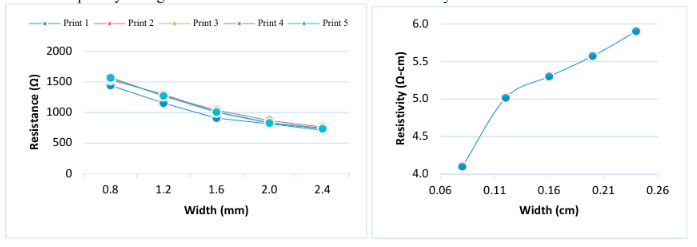
The resistivity of the 3D printed resistors varied depending on their build orientation and 3D printing process parameters.
“Resistor expansions in x axis resulted in increased resistivity, but this increase was not linear,” the researchers conclude. For z-axis expansions, the resistivity increase was mostly linear. The resistivity vs. length graph for y-axis expansion exhibited a minimum value in the middle of the test range.”
The paper offers several guidelines and recommendations for the designing and 3D printing of electrical resistors. Although the researchers used a simple design for their study, 3D printing allows for much more complex designs to be created from conductive materials and incorporated into electrical objects. As conductive materials for 3D printing start becoming more readily available, the variety of 3D printed electrical objects should expand, opening up new applications in a range of industries.
Authors of the paper include Nebojsa I. Jaksic and Pratik D. Desai.
Discuss this and other 3D printing topics at 3DPrintBoard.com or share your thoughts below.