Brazil: 3D Printing More Affordable Sensor Technology with the Piezoelectric diaphragm

Brazilian researchers outline recent scientific findings in ‘Evaluating Temperature Influence on Low-Cost Piezoelectric Transducer Response for 3D Printing Process Monitoring,’ a paper which was also presented at the 6th International Electronic Conference on Sensors and Applications last November.

Examining an alternative to the conventional acoustic emission (AE) sensor (often used in the monitoring of SLM, LMD, and FDM 3D printing systems), the authors investigate the viability of using the piezoelectric diaphragm, along with the influence of properties like temperature. Made with lead zirconate titanate, the piezoelectric diaphragm offers conductive qualities that create an electrical voltage when exposed to pressure—serving to detect mechanical changes. These sensors can be critical in operations, and the piezoelectric diaphragm is of special interest due to greater affordability in production.

“Monitoring manufacturing processes through sensors such as acoustic emission is a widely used practice nowadays,” explain the researchers. “However, the reduced cost of piezoelectric diaphragms is captivating compared to those of traditional AE sensors.”

Tests were performed on a Graber i3 desktop 3D printer, employing a heated MK2B Dual Power PCB table with NTC 100k thermistor type temperature sensor. The piezoelectric diaphragm (measuring 20 mm diameter by 0.42 mm thickness) was fixed to the table, and a Yokogawa DL850 oscillograph was used for both collection of data and storage purposes. Raw signals were analyzed both in time and frequency, and while ultimately the researchers showed that both sensors are similar, ‘it is perceived that temperature significantly influences the signal response of the piezoelectric transducer.’

(a) PLB signal; (b) Frequency spectrum for three temperatures.

“It was noted that the selected band from 400 to 500 Hz, which had the largest overlap of the spectra, presented the smallest errors, being 16.9% at 45 °C and 25.2% at 65 °C. At the same time, when comparing the errors of this band, 400 to 500 Hz, with those of the whole spectrum, from 0 to 800 Hz, an amplitude error for this band of approximately 1.6 times smaller is obtained at a temperature of 45 °C and 1.3 times lower at 65 °C, which are much smaller than those of the other selected band. Finally, the comparison of the errors between the temperatures of 65 °C and 45 °C revealed that the behavior of the errors is similar, although the errors are smaller, as expected, due to smaller temperature differences,” concluded the researchers.

3D printing is being used more often in the manufacturing of many different types of sensors and associated electronics, from ultra-modern medical wearables to microfluidics integrated with sensors to bioinspired sensors, and more.

What do you think of this news? Let us know your thoughts! Join the discussion of this and other 3D printing topics at 3DPrintBoard.com.

. (a) Mean error based on the baseline at 25 °C; (b) Mean error based on the baseline at 45 °C.

[Source / Images: ‘Evaluating Temperature Influence on Low-Cost Piezoelectric Transducer Response for 3D Printing Process Monitoring’]

The post Brazil: 3D Printing More Affordable Sensor Technology with the Piezoelectric diaphragm appeared first on 3DPrint.com | The Voice of 3D Printing / Additive Manufacturing.

3D Printing with Sensors Using Conductive ABS

In the recently published ‘3D printing of interdigital sensor based conductive ABS for salt and sucrose concentration sensing,’ authors W. Ponan and S. Harnsoongnoen outline their findings in fabricating integrated electronics.

The substrate and interdigital sensor were created with both ABS and conductive ABS filament, as the authors analyzed samples based on a direct current circuit. Because 3D printing is so centered around customization, it draws researchers, engineers, manufacturers, and users on every level who are interested in integrating electronics and completing projects more efficiently—often with ABS as their choice of material due to its conductivity.

Typically, applications include:

  • Electronic ears
  • Antennae
  • Light-emitting diodes
  • Sensors

So far, however, the authors explain that there have not been studies focused on sensor-based conductive ABS for salt and sucrose concentration sensing.

Interdigital conductive ABS sensor (a) structural layout (b) front view of fabricated sensor (c) back view of fabricated sensor (W = 4 mm, L1 = 65 mm, L2 = 70 mm and g = 2 mm).

The researchers used Esan3D Creator FDM 3D printers, with the following settings:

  • Nozzle diameter of 0.4 mm
  • Nozzle temperature of 260 °C
  • Heated platform of 60 °C

Due to the use of copper and conductive ABS, the researchers handled impedance, with the studying showing:

  • Impedance decreased with increased frequency
  • Conductive ABS with 3D printing impedance is higher than that of conductive ABS injected by 3D printing
  • Impedance of copper increased with increased frequency

In viewing the Nyquist plot for the conductive filaments, the researchers noted semi-circular impedance spectras, created from the capacitance of the conductive ABS filament. They also noted a definite connection as impedance of conductive ABS filament and conductive ABS filament injected by 3D printing increased when MUT was increased in length, resulting in impedance of all copper at 0.154 Ω. Electrical current also shifted, due to the salt and sucrose found in the deionized water concentration.

The authors listed regression value as 0.0433, with an R2 value of 0.9750.  With sucrose in deionized water, it was -0.0033, with an R2 value of 0.9594.

Percentage of solution versus electrical current (a) salt and (b) sucrose.

“We showed that the 3D interdigital sensor based conductive ABS can be used to determine the concentration of salt and sucrose. The electrical current was observed and analyzed when there were changes in the concentrations of salt and sucrose in deionized water. The proposed technique has many advantages, such as wide dynamic range, high linearity, rapid measurement and lower-cost,” concluded the researchers.

Today, 3D printing is often associated with embedded electronics, sensors, and more—to include soft robotics and other complex processes.

Researchers, manufacturers, and innovative users around the globe are integrating sensors into wearables for prosthetics, embedding them in metal 3D printing, fabricating smart fibers, bioinspired innovations, and more.

What do you think of this news? Let us know your thoughts! Join the discussion of this and other 3D printing topics at 3DPrintBoard.com.

Experimental setup (a) electrical parameter measurement (b) salt and sucrose concentration sensing.

[Source / Images: ‘3D printing of interdigital sensor based conductive ABS for salt and sucrose concentration sensing‘]

The post 3D Printing with Sensors Using Conductive ABS appeared first on 3DPrint.com | The Voice of 3D Printing / Additive Manufacturing.

3D Printed Sensors Could Be The Key to a Seamless Internet of Things

The Internet of Things (IoT) has been heralded as one of the next big steps in our technological development. The vision is somewhat utopian: the system collects information, relaying it swiftly throughout a hyperconnected network and uses that data to discover insights and take action in order to improve our daily lives. It could save energy by making devices more efficient, optimize areas like infrastructure and traffic, help with waste management and personal health, and do so much more.

The capabilities of the IoT are a result of many factors, but one fundamental aspect to consider is the sensing tech that will be used to collect data throughout IoT systems. Not only must we consider the strength and power of these sensors, but we must also consider how we are going to create such a massive amount of the devices in order to adequately track the large waves of data created out in the world.

This is where 3D printing technology and the use of nanomaterials come into play. When utilized together, they can help create the seamless and powerful IoT that we envision.

The strengths of 3D printing

3D printing is a rapidly evolving technology that has the potential to provide a great deal of value within scientific, industrial, and even everyday settings. One could viably see the technology utilized to create and mass-produce the bulk of IoT sensors. At the very least, the additive manufacturing process can help in designing optimal enclosures for the electronic components of sensors. Because of this process, it’s easy to modify or add new features to the enclosure without having to start from scratch. This flexibility would certainly benefit in the creation of sensors as they develop and change form or function.

But exciting developments in 3D printing electronic components are what will truly unlock the mass-production of strong and capable IoT sensors. The use of conductive ink — an ink for 3D printing infused with conductive materials such as copper, silver, and gold — can enable us not only to conveniently print electronics, but to also remove the constraints of the traditional 2D circuit board. By creating three-dimensional circuit boards that can take on a number of different shapes or sizes, we will be able to build a more versatile array of devices. And importantly, this can consolidate and speed up the creation of IoT sensors.

Bringing nanomaterials into play

Aside from developments in 3D printing sensors like conductive ink, we can also turn to nanomaterials, which are often cited for their high-functioning capabilities. In particular, graphene is considered an ideal material for sensors: it’s durable, flexible, highly conductive, and can detect changes in the environment through factors such as temperature, light, pressure, and can even sense chemical changes. A massive amount of research has gone into unlocking the capabilities of graphene, and its use in sensors can help provide the IoT with accurate information and greater resilience.

This means that it can address both the external and internal needs of IoT sensors (i.e. the creation of a strong and resilient enclosure and of highly capable electronic parts). And seeing as how 3D printing could be instrumental for enabling the creation of sensors on a far greater scale, it stands to reason that pairing this process with graphene would be an immense boost to the capabilities of an IoT system.

IoT sensors, in order to provide accurate measurements on the environment around them, must be strong enough to withstand harsh conditions such as rain and snow, or some industrial cases, be strong enough to withstand extreme heat or even salt erosion from marine-based applications. For more traditional metals and materials, the elements could quickly wear at the tech, which could result in inaccurate data that would disrupt the IoT system. It would also be highly inefficient to constantly replace sensors, making durable nanomaterials as the ideal base for creating sensors.

Fighting headwinds and promising developments

But the other hurdle to overcome revolves around the sheer number of sensors that we’ll need to run IoT systems. Market researchers estimate that there are already more than 20 billion connected devices in today’s world, and that number will only continue to grow as we become more technologically advanced and seek to bring about a true IoT. The sheer number of devices translates to an equally massive amount of sensors, and making advanced, nanomaterial-based sensing tech for widespread use is a monumentally challenging endeavor, especially as mass-producing nanomaterials like graphene have proven difficult in the past. In addition, the cost of implementing so many sensors may give many pause over pursuing such a cause, even if the nanomaterial-based sensors are so capable.

The “wonder material” graphene, which has historically been troublesome to produce, has recently seen potential breakthroughs that will allow scientists to create higher quantities, which in the case of 3D printing IoT sensors means that printers could very well have plenty of material to work with.

SEM images of Graphene Oxide ink

Scientists have also recently experimented with 3D printing objects with graphene, which could prove to be the final key in unlocking nanomaterial-based sensors for the IoT. Researchers in China have discovered a way to utilize the virtually 2D material to create 3D objects by using a graphene oxide ink, and have successful used the nanomaterial to create tiny supercapacitors.

Graphene-based cilia inspired sensors.

It’s not far-fetched to say that if graphene ink can be used to 3D print batteries, sensor tech can’t be too far behind. For instance, graphene has been used to 3D print biologically-inspired cilia sensors that imitate how creatures in nature sense their surroundings. Paired with other developments in printing sensor tech, such as integration with wearables, the scientific world has taken a massive step toward making the process of mass-producing nanomaterial-based sensors faster and more affordable.

The development of sensing tech and the need to overcome the various obstacles in their creation and implementation are issues that seem to fly under the radar when discussing the amazing possibilities presented by the Internet of Things. But in spite of these challenges, the IoT is purported to hit the mainstream by 2020. And when looking at the trajectory of 3D printing and nanotechnology for sensor use, it’s clear that we are well on our way to achieving a seamless sensor-based IoT.

Don Basile is a Venture Capitalist and writer and you can find him here.

The post 3D Printed Sensors Could Be The Key to a Seamless Internet of Things appeared first on 3DPrint.com | The Voice of 3D Printing / Additive Manufacturing.

London: 3D Printing the Double-Ridged Horn Antenna for Biomedical Monitoring

Researchers are looking into ways to optimize biomedical monitoring, with their results outlined in ‘A 3D Printed High-Dielectric Filled Elliptical Double-Ridged Horn Antenna for Biomedical Monitoring Applications.’ Seeking to make further impacts in the field of medical science, the team from Queen Mary University of London has 3D printed an innovative device for sensing applications with wireless technology—based on ultra-wideband devices initially created for short-range wireless communications.

The in-house measurement setup based on the open-ended coaxial probe technique, used for the characterization of the dielectric materials.

Created to work within UK Communications Industries (Ofcom) and the Federal Communications Commission (FCC) regulation of UWBs, the new device has been found to offer depth suitable for penetration in scanning skin, muscle, and fat, with signals able to sense layer thicknesses. Wide-band technologies are often used for short-range communication due to:

  • Low power
  • High data rates
  • Multipath immunity
  • Simultaneous ranging and communication

While this type of antenna is not new, the use of 3D printing is novel. The double-ridged horn has been a topic of research over the years for researchers because of the benefits, leading to a more effective answer to refining accuracy in biomedical scanning. And while 3D printing can offer greater affordability in many cases, here the research team was concerned about cost-prohibitive fabrication, so they compared materials, ultimately settling on in-house 3D printing with ABS.

The shape of the horn allows for better operation overall, and the high dielectric material allows for a miniaturized design that also reduces reflection and is both easy and affordable to make. With an extension, the scientists were able to expand on the antenna and prevent signal-overlapping issues.

Modeled extended EDRH antenna with the structural labels and the dimensions for the extended section.

“The optimal approach is to extend the outer aperture of the antenna, and to define, the antenna outer aperture length, so the scanning tissue area can be placed in the far-field region,” stated the researchers. “This has added more complexity to the fabrication and realization of the device with the increased cost, but on the other hand, it has made it more stable in its operation, and free of any destructive interference signals and noise.”

The team used the Stratasys Objet30 Prime 3D printer for creating their prototype, finishing it with clear Vero polyethylene, stating that hardware and materials not only offered high resolution, accuracy, and conductivity, but also affordability in fabrication.

Measurements were found to be accurate also, as they addressed concerns regarding individual and other influences like scanning areas and layer structure but concluded that there should be very little variance between ‘permittivity and thickness.’ If an impact on the results was noted, the researchers explained that added calibration measures could be taken with an open-ended probe, with software producing the results.

(a) 3D-printed EDRH antenna using the polyethylene material. (b) 3D-printed EDRH antenna, as conductive-painted and fed with a semi-ridged SMA connector. (c) 3D-printed EDRH antenna filled with the high-dielectric mixture.

“This design incorporates the extension for locating the antenna in the far-field region of the scanning area, for the plane-waves to penetrate more directly into the body. Moreover, the antenna can operate at the lower frequency band of WB to exhibit a better penetration depth and impedance matching using the mixture for the biomedical application, which monitoring very deep inside the body is the main objective of the system,” concluded the researchers at the end of their study.

3D printing has offered much greater expansion opportunities for scientists and engineers interested in creating better devices for sensing and monitoring, from automotive sensors to electrochemical sensing, and 3D printed models for better monitoring.

What do you think of this news? Let us know your thoughts! Join the discussion of this and other 3D printing topics at 3DPrintBoard.com.

[Source / Images: ‘A 3D Printed High-Dielectric Filled Elliptical Double-Ridged Horn Antenna for Biomedical Monitoring Applications’]


The post London: 3D Printing the Double-Ridged Horn Antenna for Biomedical Monitoring appeared first on 3DPrint.com | The Voice of 3D Printing / Additive Manufacturing.

International Researchers Review Methods for 3D Printing Biomedical Sensors

Researchers from both China and India have come together to review the current 3D printed sensor scene, regarding the technology being used and applications and industries being impacted. Authors Tao Han, Sudip Kundu, Anindya Nag, and Yongzhao Xu published their findings recently in ‘3D Printed Sensors for Biomedical Applications: A Review.’

While manufacturing of sensors has continued to progress, obstacles have prevailed, and in many ways have stalled sensor fabrication from achieving its true potential in many applications. As the authors point out, sensors are all around us, but many are limited due to the cost involved in manufacturing, challenges regarding materials (such as silicon, also posing problems at low frequencies), and issues with temperature. More importantly, most sensors are not biocompatible, thus stilting advances in the medical arena.

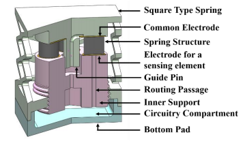
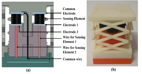
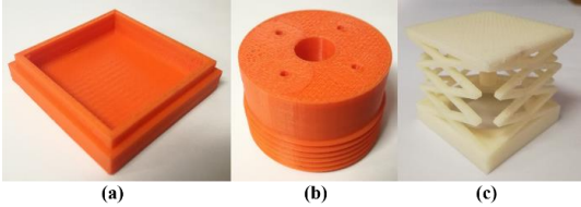
With the advent of 3D printing, sensors can be designed in a more streamlined and affordable process, involving less steps in production and less hours needed in labor for creating accurate prototypes that can then be made digitally. 3D printed sensors are usually much stronger and more durable too and have shown promise for monitoring blood pressure and heart rate, respiration, temperature, brain activity, and more.

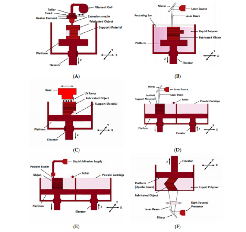
(A) Fused deposition modelling (B) Stereo-lithography (C) Polyjet Process (D) Selective laser
sintering (E) 3D Inkjet printing (F) Digital light processing.

Currently, the following processes have been used to make sensors successfully:

  • Fused deposition modelling (FDM)
  • Stereolithography (SLA)
  • Polyjet process
  • Selective laser sintering (SLS)
  • 3D inkjet printing and DLP

“Among these six types, the most common type is the FDM one, which has been largely used to develop prototypes for electrochemical sensing purposes,” state the researchers. “Others like FDM, SLA and ink-jet printing have also been considered for forming prototypes since they can be developed with lower resolutions. Polyjet and SLS processes are mostly used for forming sensors which are employed for cell culture applications.”

FDM 3D printing has been popular among users for biomedical uses, with both AB and PLA materials, as well as alternatives like waxes and nylon. Bioprinting has also been successful, with researchers noting good cell viability and sustainability. The authors note, however, that disadvantages in using FDM 3D printing include lack of shape integrity and leakage when materials are not ‘properly tuned.’ Sensors have, however, been created for detecting glucose, cancer biomarkers, and other items like reactors for biological sample monitoring.

SLA 3D printing is useful due to its ability to create large-scale items. Researchers have used ABS to create more complex devices like biosensors and microfluidic devices for detecting pathogens. Disposable and portable electrochemical sensors have also been created, along with intricate components like a 3D printed microfluidic part for urinary protein quantification, comprised of a pushing valve, rotary valve, and torque-actuated pump.

a) Schematic illustration of separation of the captured bacteria by inertial focusing. (b)
Representation of dean vortices in a channel with trapezoid cross-section. (c) Photograph of the 3D
printed microfluidic device. Reproduced from Lee et al. [112].

In polyjet printing, a curing or hardening process creates parts—and like in FDM 3D printing, multiple nozzles can be used.

“Since multiple jetting heads are used for printing, this allows building multi-colored objects in a single structure. One of the main advantages of this process is that a high resolution of 16 µm can be achieved for the prototypes, having an accuracy of less than 0.1 mm.”

Using polyjet 3D printing, cell viability sensor-based fluidic devices have been created, along with other innovations such as leak-proof 3D printed storage devices. Other sensors have been created through polyjet 3D printing for ATP and dopamine sensing, along with physiological sensors, and electrochemical and biocompatible sensors.

SLS printing is used in AM processes with the use of metal powders:

A certain laser power is required to melt the periphery of the particles using the localised energy of a laser beam. The unused powder acts as a support structure for the 3D printed part. After scanning each layer, the structure is lowered to spread a new powder layer which can be scanned according to the computer-aided design (CAD) design. Not only metallic powder particles but also ceramics and polymers or combinations with each other can be used in SLS,” state the researchers.

Benefits in SLS 3D printing are that many different materials can be used—and precisely so—with powder available for recycling. Cell density sensors have been created, explain the authors, and they could be extended to manipulate cell ‘disruptions,’ distribute chemicals, and control enzymatic assays.

. Continuous recalibration of the 3D-printed Control Unit Adaptive P controller. Reproduced from Ude et al. [127]. (A) The 3D printed flask is used to control the pH of the solution using defined algorithm. (B) The interior of th3 3D printed flask. (C) Variation in the amplitude, pH levels and intensity of the scattered light with time.

3D inkjet printing offers benefit in creating strong, complex structures; for example, researchers have been successful in creating items such as a 3D printed bionic ear. Others have created items like actuator integrated heart structure-shaped 3D elastic multifunctional biomembranes for sensing spatial and temporal responses.

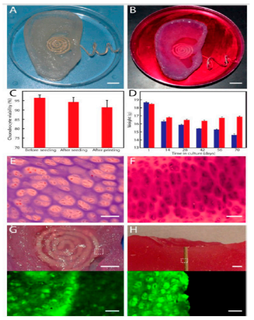
Image of the (A) fabricated 3D printed bionic ear and (B) 3D printed bionic ear during its vitro culture. (C) The viability of chondrocyte at different stages during the printing process. (D) Deviation of the weight of the printed ear over time in culture, where the ear consisted of the chondrocyte-seeded alginate or only alginate shown in red and blue colour respectively. (E) Histologic analysis of chondrocyte morphology done using H&E staining. (F) Neocartilaginous tissue
being Safranin O stained after 10 weeks of culture. Photographs (top) and fluorescent (bottom) images of (G) viability of the neo cartilaginous tissue being in contact with the antenna of the coil and (H) cross-section of the bionic ear showing the viability of the internal cartilaginous tissue in contact with the electrode. Reproduced from Mannoor et al.

DLP 3D printing is like that of SLA, but a projector screen flashes, projecting layers like images:

“Each 2D hardened layer is formed after exposing the liquid polymer to projector light under the safest conditions instead of making a layer with several laser scan paths,” state the researchers. “The process is repeated until the entire structure is fabricated.”

Items such as glucose biosensors, light-addressable potentiometric sensors, and semiconductor-based biosensor are a few devices that have been created so far with DLP 3D printing.

“Each of these processes has its own merits and demerits related to cost and time of fabrication, the type of materials that can be processed and prototypes that can be formed,” concluded the researchers. “A few of the current bottlenecks have also been mentioned, along with the possible remedial solutions to deal with them. Finally, a market survey has been presented about the expenditures on the different types of 3D printing techniques in the current scenario and in the upcoming years to develop sensors and other electronic appliances.”

3D printing has made a significant impact in the realm of electronics, however, and even more specifically, sensors. Over the years, we have followed a wide array of sensors created to improve monitoring and functionality in numerous applications, from fending off 3D printing cyberattacks to fabricating fiber optics or tending to simple but scientific matters like measuring the water intake of plants. What do you think of this news? Let us know your thoughts! Join the discussion of this and other 3D printing topics at 3DPrintBoard.com.

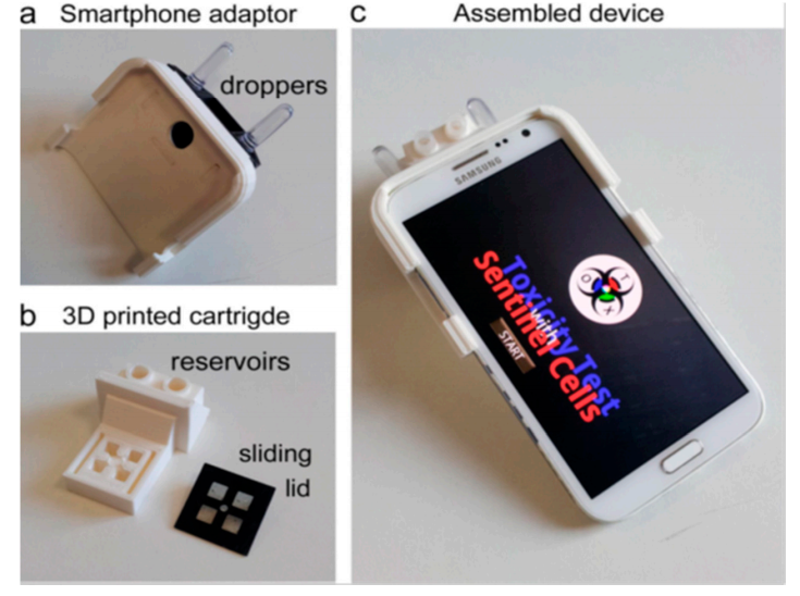
(a) A 3D printed smartphone adaptor depicting its (b) 3D printed cartridge being composed
of reservoirs and sliding lid. (c) The assembled smartphone-based device for BL signal acquisition
and analysis. Reproduced from Cevenini.

[Source / Images: 3D Printed Sensors for Biomedical Applications: A Review]

Research Group Creates 3D Printed Sensor that Changes Color When Exposed to Wet Conditions

In the dry state (left; in an anhydrous liquid), the sensor material is purple; in the wet state (e.g. from air humidity) it turns blue. These 3D printed workpieces are each about one centimeter wide. [Image: Verónica García Vegas, UAM]

A collaborative group of scientists from the Autonomous University of Madrid (UAM), the Hebrew University of Jerusalem, the Nanyang Technological University in Singapore, the Institute for Materials Science in Madrid (ICMM-CSIC), and the Deutsches Elektronen-Synchrotron (DESY) worked together to develop a versatile 3D printable sensor, made of an inexpensive plastic-composite, that can detect tiny amounts of water and change color in wet conditions.

The team, led by UAM’s Pilar Amo-Ochoa, developed the flexible, non-toxic material, which will change from purple to blue when exposed to moisture, and detailed their work in a research paper, titled “3D Printing of a Thermo- and Solvatochromic Composite Material Based on a Cu(II)–Thymine Coordination Polymer with Moisture Sensing Capabilities,” that was recently published in the journal Advanced Functional Materials.

The abstract reads, “This work presents the fabrication of 3D‐printed composite objects based on copper(II) 1D coordination polymer (CP1) decorated with thymine along its chains with potential utility as an environmental humidity sensor and as a water sensor in organic solvents. This new composite object has a remarkable sensitivity, ranging from 0.3% to 4% of water in organic solvents. The sensing capacity is related to the structural transformation due to the loss of water molecules that CP1 undergoes with temperature or by solvent molecules’ competition, which induces significant change in color simultaneously. The CP1 and 3D printed materials are stable in air over 1 year and also at biological pHs (5–7), therefore suggesting potential applications as robust colorimetric sensors. These results open the door to generate a family of new 3D printed materials based on the integration of multifunctional coordination polymers with organic polymers.”

3D printed sensors have many potential uses, such as cardiac research, an early warning system for wildfires, and other water-related applications, like determining how much water a plant is using. But the demand is increasing across many industries for responsive sensors that can quickly change, in a simple way, when they are exposed to specific molecules…such as water, which is one of the most common chemicals monitored by these types of sensors.

“Understanding how much water is present in a certain environment or material is important. For example, if there is too much water in oils they may not lubricate machines well, whilst with too much water in fuel, it may not burn properly,” explained scientist Michael Wharmby, a co-author of the paper and head of DESY’s beamline P02.1.

DESY, a national research center in Germany, operates particle accelerators, and the team examined their new sensor material with the X-ray light source PETRA III at Wharmby’s beamline. Using X-rays to investigate the material allowed the team to better understand the internal structural changes that water triggers, which lead to the color change.

Additionally, these high energy X-rays revealed that the functional part of the material – the versatile copper-based coordination polymer – was in fact working.

José Ignacio Martínez, a co-author of the paper from ICMM-CSIC, said, “Having understood this, we were able to model the physics of this change.”

This compound, known as CP1, consists of a water molecule that’s bound to a central copper atom. Once the sample is heated i[ to a certain temperature, the water molecule is removed, which then leads to the material going through a reversible structural reorganization that ultimately causes the color to change.

“On heating the compound to 60 degrees Celsius, it changes colour from blue to purple. This change can be reversed by leaving it in air, putting it in water, or putting it in a solvent with trace amounts of water in it,” explained Amo-Ochoa.

Front and side views of the computed optimal geometries for the compound CP1

Then the team mixed the copper compound into a 3D printing ink, which they used to 3D print sensors in a variety of different shapes. The sensors were tested in the air, and also with solvents that contained different amounts of water, which revealed that the porous objects were even more sensitive than the compound itself to the presence of water.

The 3D printed sensors were able to detect 0.3 to 4% of water in solvents in less than two minutes, while they could detect a relative humidity of 7% in air. If the material is dried, either through heating or in a water-free solvent, it will return to purple. The team’s research showed that the material will remain stable over many heating cycles, and that it remains stable in the air for at least one year, at biologically relevant pH ranges of 5 to 7. Additionally, the copper compounds are shown to be evenly distributed throughout each sensors.

Co-author Shlomo Magdassi from The Hebrew University of Jerusalem said that the team’s concept could eventually be used to create additional functional materials in the future, for use in a wide range of industries.

“This work shows the first 3D printed composite objects created from a non-porous coordination polymer. It opens the door to the use of this large family of compounds that are easy to synthesize and exhibit interesting magnetic, conductive and optical properties, in the field of functional 3D printing,” said co-author Félix Zamora from UAM.

Co-authors of the paper are Noelia Maldonado, Verónica G. Vegas, Oded Halevi, Martínez, Pooi See Lee, Magdassi, Wharmby, Ana E. Platero-Prats, Consuelo Moreno, Zamora, and Amo-Ochoa.

Discuss this research and other 3D printing topics at 3DPrintBoard.com or share your thoughts in the Facebook comments below.

[Source: EurekAlert]

3D Printing Used to Develop Tactile Sensor

Tactile sensors are used in the development of robotics, computers and security systems. They are often used in touchscreens, as well as to mimic the human sense of touch for robots. In a paper entitled “Design and Development of a Conductive Polymer Based 3D-Printed Tactile Sensor with Square Type Spring Structure,” a group of researchers describe their creation of a tactile sensor using 3D printing.

Conductive polymer-based piezoresistive tactile sensors enable a flexible quality which is present in human skin; however, according to the researchers, most of these tactile senors are unable to identify more than two parameters simultaneously. In the study, the researchers designed, developed and tested a tactile sensor with the dimensions of 50 x 50 × 56 mm based on a 2×2 conductive polymer based sensing element array incorporated to a square type spring structure. This spring structure was produced using 3D printing.

The sensing element was developed to be highly customizable. The sensor’s base material is silicone rubber which has enhancements by silica and carbon black, with Silane as the coupling agent.

“The spring structure stated in this paper has been designed for force scaling purpose and numerically analyzed using COMSOL Multiphysics prior to the fabrication,” the researchers state. “Circuitry for embedded electrodes was also developed in this research with a wireless communication between the sensor assembly and the developed user interface which allows to use the sensor as a plug and play device.”

With force sensors, it is necessary to define a working range. Controlling the working range can be done by overseeing the deflection applied to the sensing element. By introducing an external square type spring structure to sensing elements, the working range can be easily altered. The spring structure is designed to facilitate a 2 x 2 array of sensing elements and designed for three separate parts.

A two-layered saw tooth shape was developed in a single square type spring, which was 3D printed using ABS Plus. The fabrication of the sensor itself was carried out in two stages: the fabrication of the sensing element and then the sensing structure. The sensing element was made mostly from Room Temperature Vulcanization (RTV) Silicone Rubber. A mechanical molding method was used to create the sensing element, with the mold designed in three layers to make the sensing element easier to remove.

“The mould is capable of developing sensing elements with different geometries and with different thickness ranges in one batch of production,” the researchers explain. “A key feature of this production process is sensing elements can be developed according to the required geometry and size with different performance levels.”

Three parts in total were 3D printed; the square type spring structure was printed in ABS with 100% infill while the other two parts – the bottom pad and the inner support – were printed with PLA with 75% infill. The sensing element was then tested using a static load test.

“This square type spring structure minimized deflection of the sensing element while it allows the expansion to the operation range,” the researchers conclude. “This sensor designed to overcome the inherent issues in conductive polymer based sensing elements using an internal signal conditioning circuitry.”

Discuss this and other 3D printing topics at 3DPrintBoard.com or share your thoughts below.