IDS Releasing Aerosol-Based Desktop Electronics 3D Printer at NextFlex Innovation Day

Coming up on August 8th, the NextFlex consortium will be holding an Innovation Day at its San Jose, California headquarters. The invitation-only workshop (request an invite here) celebrates the progress made on projects and results achieved in the Technology Hub, in addition to giving members a way to discover new technology, network with each other, and meet influencers in the FHE (Flexible Hybrid Electronics) manufacturing supply chain. This year, New Mexico-based company IDS will be on hand at the event to officially announce the release of its updated desktop aerosol 3D printer.

IDS, which stands for Integrated Deposition Solutions, is a small business in Albuquerque. Founded in 2013, the company is looking to become a leader in the field of 3D printed electronics – it has licensed an aerosol-based AM technology, called NanoJet, from Sandia National Laboratories and adapted it for Direct-Write Electronic (DWE) 3D printing.

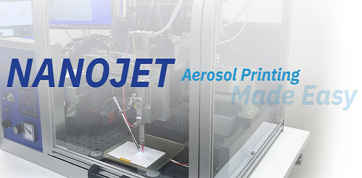
According to IDS, the company’s updated desktop 3D printer is a high-performance, low-cost system for aerosol 3D printing applications, such as printed electronics. IDS claims it’s the “first affordable aerosol-based print platform” in printed electronics that’s currently available for both research purposes and low volume production.

“The NanoJet technology is cost-effective, easy to use, reliable and capable of operating for extended periods of time without operator intervention,” the IDS website states. “The ability to print features from approximately 10 µm to 200 µm in width in conductors, dielectrics, resistors and other electronic specific materials makes the aerosol-based NanoJet technology unique.”

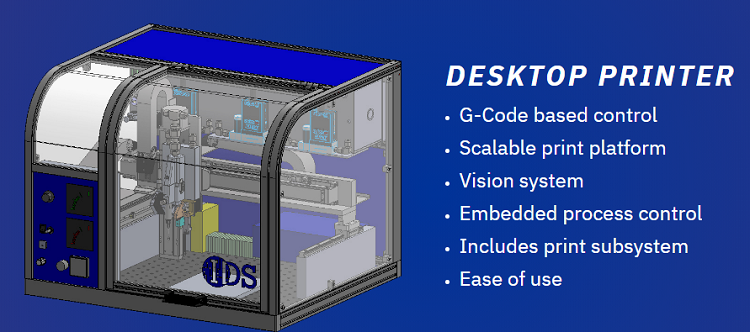
IDS’ aerosol 3D printer has integrated its reliable NanoJet technology into a functioning desktop machine, which includes a process vision system, print process controls, simplified tool path generation, and industrial motion control driven by G-code. This motion control platform provides flexibility to end users in using tool path generators, whether it’s the one that came with the IDS printer or something similar. In addition, the multiple NanoJet print heads make it easy to switch materials between development, production, and and research processes, thanks to its aerosol focusing assemblies and easy to replace ink cartridges; each print head includes its own module.

The printer also has a 150 x 150 mm heated platform and point of use aerosol generation. Applications for IDS’ aerosol-based NanoJet 3D printing include:

  • biomedical
  • conformal electronics
  • high-density interconnects
  • wireless power transfer

Another company that’s well-known for using an aerosol-based 3D printing process is production-grade 3D printer supplier Optomec, with its patented Aerosol Jet technology for 3D printing electronics. Aerosol jetting is a very important technology because of its ability to create intricate products like antennae and sensors.

I’m not sure if IDS’ technology works the same as Optometc’s aerosol 3D printing, but I would bet the processes are very similar. IDS claims its desktop system is a plug-and-play 3D printer, with continuous operation for four hours of unattended printing, that uses Ag nanoparticle ink and single pass line thickness between 100 nm to 4 µm. The company also says that its aerosol 3D printer costs three times less than other commercially available aerosol-based systems; you can contact IDS for a quote.

What do you think? Discuss this story and other 3D printing topics at 3DPrintBoard.com or share your thoughts in the Facebook comments below. 

[Images: IDS]

The post IDS Releasing Aerosol-Based Desktop Electronics 3D Printer at NextFlex Innovation Day appeared first on 3DPrint.com | The Voice of 3D Printing / Additive Manufacturing.

Samsung Electronics Using Optomec’s Aerosol Jet 3D Printing to Make Next-Generation Consumer Electronics

New Mexico-based Optomec, which supplies production-grade 3D printing systems for electronics applications and LENS Directed Energy Deposition 3D printers for the manufacturing of metal parts and components, just announced that Samsung Electronics will be using its patented Aerosol Jet technology. This week, it was revealed that Samsung has commissioned one of Optomec’s Aerosol Jet (AJ) 5X 3D printers, which will be put to work in its Printed Electronics Lab for the fabrication of next-generation consumer electronics.

First unveiled back in 2014, the AJ 5X was developed for those customers working to develop electronics like molded interconnect devices (MIDs), sensors, smart phones, and tablets. Many customers use the system to work on more advanced fabrication projects, as it has the ability to print high conductivity inks and dielectric materials in complex shapes on a variety of substrates and 3D surfaces, which makes it possible to shrink electronic devices down.

[Image: Optomec]

Optomec’s Aerosol Jet technology accurately and precisely deposits electronic inks through the use of aerodynamic focusing. First, the material is place into an atomizer, which creates a mist of ink-laden droplets that is delivered to the deposition head. There, a sheath gas (usually compressed air or clean, dry Nitrogen) surrounds the aerosol as an annular ring to focus it. Once this gas and the aerosol pass through the profiled nozzle, acceleration occurs and the aerosol is focused into a tight stream of droplets that flow inside the gas, which also insulates the nozzle to prevent any material clogs.

“The resulting high velocity particle stream remains focused during its travel from the nozzle to the substrate over a distance of 2 to 5 mm maintaining feature resolution on non-uniform and 3D substrates,” the Optomec website states. “The system is driven by standard CAD data which is converted to make a vector based tool path. This tool path allows patterning of the ink by driving a 2D or 3D motion control system. Printed features range from 10 microns to millimeters.”

The Optomec AJ 5X system can print features that range from millimeters down to 10 microns, and the 3D printer also supports 5 axes of coordinated motion with its 200 x 300 x 200 mm print envelope. The company has 20 years worth of materials and process research to its name, can help industry customers improve performance and lower product costs, and it also offers the necessary software to go with its Aerosol Jet systems for printed electronics.

The patented Aerosol Jet process is used by many to make things like sensors, RF interconnects, flexible hybrid electronics, wire replacement bonds for IC packaging, and multi-layer, miniature circuits; the technology can even be used to 3D print antennas directly onto electronics enclosures.

Discuss this story and other 3D printing topics at 3DPrintBoard.com or share your thoughts in the Facebook comments below.

[Source: Optomec]

Researchers Use Aerosol Jet 3D Printing to Develop Neuronal Interface with More Anti-Inflammatory Ability

a) Schematic illustration of the mechanism for formation of nanogel-based membrane based on the self-assembly of OPC-incorporated amphiphilic polydimethylsiloxane-modified N, O-carboxylic chitosan (OPMSC), followed by hydrogel-bonding interaction of OPC. The TEM images display the network structure of b) PMSC and c) OPMSC spherical nanogels.

3D printing has been used in the past to help treat degenerative diseases, or at least make it easier to cope with them. In terms of neurodegenerative diseases, implanted prosthetic devices are often used, but adverse biological reactions in host tissues can result in signal failure. it’s important to create tissue that can mimic the mechanical and structural properties of neural implanted devices, and while flexible polymer-based implants have helped to alleviate some injuries, the mechanical stress doesn’t quite match brain tissue. That’s why a lot of research has been conducted about using conductive polymer (CP) composites or conductive hydrogels to coat the devices so the biocompatibility and electrochemical performance of neural electrodes can be improved.

Representative fluorescent images demonstrate tissue responses around the tip of the non-coated probe and the OPMSC-coated probe at days 2, 7, 14, and 28 post-implantation. (c) ED1 staining; (e) GFAP staining; (g) NeuN staining.

But, a team of researchers from China and Taiwan say that it’s more important to design biocompatible coatings for implanted devices that mimic mechanical and structural properties of brain tissues, so tissue responses after long-term utilization can be reduced.

The researchers believe that 3D nanostructural coatings should be developed for the insulated regions, and not the implant electrode sites, so implants can interface with nearby brain tissues with more stability. They explained their findings in a recently published paper, titled “Multifunctional 3D Patternable Drug-Embedded Nanocarrier-Based Interfaces to Enhance Signal Recording and Reduce Neuron Degeneration in Neural Implantation.”

“Although the nanomaterial-based substrate coatings incorporated into drug delivery systems such as poly(lactic-co-glycolic acid) (PLGA) nanoparticles, pHEMA, or PLGA nanoparticles-embedded matrix have been developed, these systems lack stable physical and chemical properties for reducing tissue responses, including an appropriate nanostructural interface, mechanical properties, and biofouling ability,” the researchers wrote. “Multifunctional drug-embedded coatings must be developed and integrated into the nanostructural neural interfaces to allow sustained release of bioactive molecules (anti-inflammatory drugs) and simultaneous construction of a brain tissue-mimic but bioinert microenvironment for reducing both acute and chronic inflammation reactions during long-term implantation.”

The researchers used aerosol jet 3D printing to develop a neuronal interface with prolonged anti-inflammatory ability, structural and mechanical properties that mimicked brain tissue, and a sustained nonfouling property in order to inhibit tissue encapsulation.

Using aerosol jet printing, the OPMSC suspensions were directly patterned on a neural probe to create an anti-inflammatory neural interface.

“With the integration of nanomanufacturing technology and multifunctional nanomaterials into the neural implants, we can extensively reduce the reactive tissue responses, provide continuous protection of surviving neurons, and ensure long-term performance reliability of implants,” the researchers explained.

They created a new 3D nanocarrier-based neural interface that could possibly be used to support long-term neural implantation, as well as achieve better therapy for chronic and degenerative diseases. The researchers used a “novel combination of antioxidative zwitterionic nanocarriers and nanomanufacturing technology” to make the interface. The team developed a new type of anti-inflammatory nanogel, based on the amphiphilic polydimethylsiloxane-modified N, O-carboxylic chitosan (PMSC) incorporated with oligo-proanthocyanidin (OPC), called OPMSC.

a) Optical microscopy image showing patterning morphology of PMSC and OPMSC arrays with a thickness of ≈30 µm obtained by aerosol jet printing. The red arrows indicate the patterned location. Comparison of PC12 cell patterning on b) PMSC and c) OPMSC arrays demonstrates that OPMSC can maintain structural stability in a biological microenvironment. d) An overview and SEM images of the flexible OPMSC-coated polyimide probe. e) SEM image showing a cross-sectional view of OPMSC-coated probe after washing with water.

“The natural OPC can be used as an anti-inflammatory drug due to its multipotent therapeutic effects on neurodegenerative diseases,” the researchers explained. “Furthermore, given the abundance of hydroxyl groups and the aromatic architecture, the semi-hydrophilic OPC can act as a structural stabilizer to help the self-adhesion of nanogels, making the structure evolve into a biostable 3D anti-inflammatory neural interface.”

The team directly fabricated OPMSC nanogels onto a membrane using aerosol jet printing technology, because it is a low-temperature technology. When developing neural implants, mechanical properties are the main concern, which is why the researchers conducted a tensile test, among other experiments, on their new 3D nanocarrier-based neural interface, which was also implanted into rodents.

“After short-term and long-term in vivo implantation, the OPMSC-coated neural probe displayed a relatively lower impedance value and much higher signal stability compared to noncoated probe,” the researchers concluded. “The ADC obtained by magnetic resonance imaging (MRI) demonstrated that the OPMCS-coated probe alleviated edema at the acute phase, and further reduced tissue trauma in the chronic phase. Immunostaining of anti-NeuN, anti-ED1, and anti-GFAP around the implanted site further demonstrated that the OPMSC-coated probe significantly reduced the population of activated microglia and astrocytes for all durations, resulting in increased survival 28 d after implantation. Such multifunctional nanostructured OPMSC-coated neural probes can provide a long-lasting functional neural interface for long-term neural implantation.”

Co-authors of the paper are Wei-Chen Huang, Hsin-Yi Lai, Li-Wei Kuo, Chia-Hsin Liao, Po-Hsieh Chang,Ta-Chung Liu, San-Yuan Chen, and You-Yin Chen.

Discuss this and other 3D printing topics at 3DPrintBoard.com or share your thoughts below.