New 3D Printing Resin Made with Nanodiamond Powder

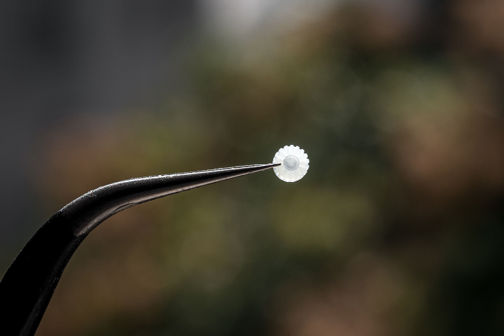
Nanodiamonds are diamond particles produced by explosions, and are very thermally conductive. Nanodiamond powder is made up of non-toxic diamond nanoparticles, with a large surface, that are about 5 nm in size, and feature some interesting properties.

Researchers Krzysztof Królewski, Aleksandra Wieloszyńska, Aleksandra Kamińska, and Katarzyna Kardacz from Poland’s Gdańsk University of Technology (GUT), wanted to investigate a particular property, and published a paper on their work, titled “Optical properties of daylight curable resin doped with nanodiamond powder.”

The abstract reads, “In this paper a new material for 3D printing was elaborated on. Since diamond has very good optical properties, an idea occurred to us to apply it in a 3D printing process. A mixture of nanodiamond powder and standard 3D printing resin was created and several printouts have been completed. They have been tested for their abilities to transmit and absorb light in a wide spectrum of wavelengths. It turned out that nanopowder doped resin in comparison to standard one has worse optical properties. However, it shows that a mixture of resin and nanopowder can control optical properties of printouts.”

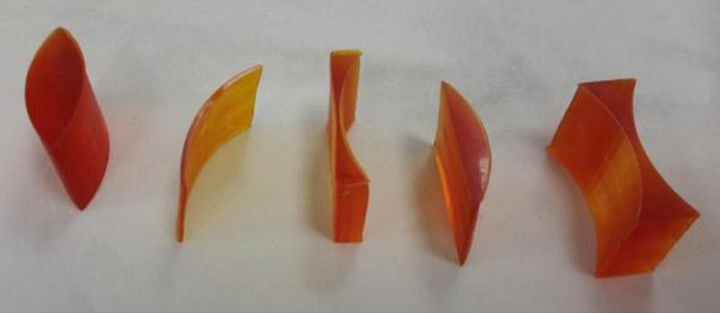
Fig. 1. Prototypes of 3D printed cylindrical lenses. L-R: convexo-convex lens, convexo-concave lens, plano-concave lens, plano-convex lens, and concavo-concave lens.

The team prepared and analyzed a new 3D printing material made out of diamond nanoparticles and amber 3D Daylight Hard resin from Photocentric, which caused unique optical properties. They fabricated a few examples of their material on the Liquid Crystal 10′ 3D printer, and then tested the optical properties, along with the optical properties of the Photocentric polymer resin for comparison.

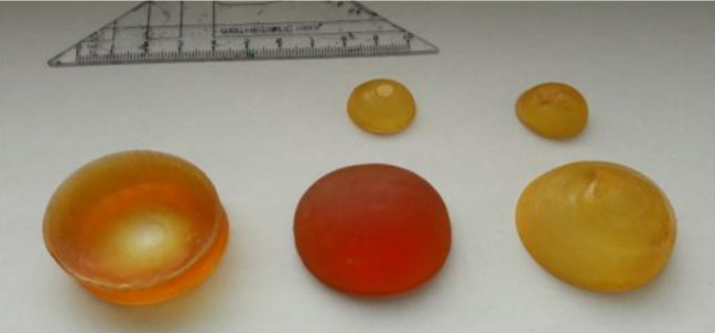
Fig. 2. Prototypes of 3D printed spherical lenses. Bottom L-R: plano-concave lens, plano-convex lens, and convex-concave lens. The top row shows two convex-concave lenses.

“The 20 mm × 20 mm plates were printed as test samples which were prepared with different thickness (0.2 mm, 0.5 mm, 0.8 mm, 1 mm, 1.5 mm, 2 mm and 5 mm),” the researchers explained.

A spectrometer was used to obtain transmission characteristics of the 3D printed sample plates, in the 200-1100 nm wavelength range at room temperature. These characteristics are defined by, as the researchers wrote, “increasing transmission with decreasing the thickness of plates.”

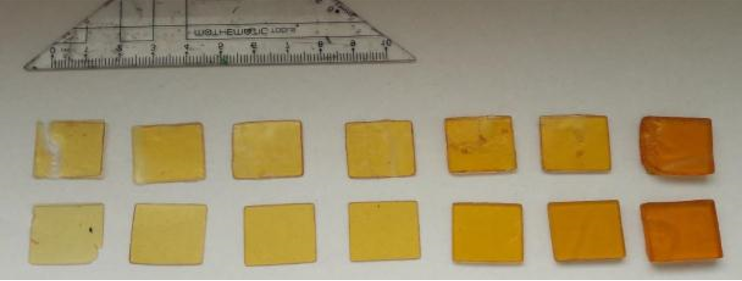
Fig. 3. Two series of flat plates (first series at top and second at the bottom). The thinnest plate is on the left.

For the first series of 3D printed plates, the transmission was almost zero for light waves in the 200-400 nm range, while the greatest transmission was for those in the 800-1100 nm range. The transmission for series #2 was even higher, which was easy to see with thicker plates. These characteristics are comparable with those of other optical materials, such as fused silica, and are definitely appropriate for a number of optical applications.

“In the first series, the maximal transmission is 60% and 44% for 2 mm and 5 mm thick plate, respectively. In turn, in the second series, this value is 75% and 65%, respectively,” the researchers noted.

The team then determined the absorption characteristics for the plates, and found that the greatest absorption is for light waves in the 200-400 nm, due to their orange color; the lowest absorption was for waves in the 600-1100 nm range.

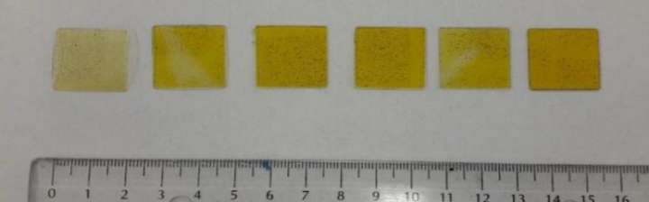
Fig. 8. One series of flat plates, printed from the mixture of resin and nanodiamond powder which was obtained by evaporating DMSO from the suspension with nanodiamond.

More plates were then 3D printed out of the team’s novel material of nanodiamond powder and resin. The researchers then went into a little more detail as to how they obtained, and created, the material.

“The nanodiamond powder was obtained by evaporating DMSO (dimethyl sulfoxide) from the suspension with nanodiamond,” they wrote. “Then the 66.835 g liquid resin was mixed with 0.069 g powder. First, the magnetic stirring was carried out for an hour and after that, the sonication was done for 45 minutes. The sonicator worked in pulse mode with power set at 10%.”

The team used a series of OCT measurements to evaluate the material properties of the 3D printed plates, and got single B-scans from three plates with diamond nanoparticles, and one without, for reference. The images show that because of nanoparticles being present, and “the lack of tendency to agglomeration,” the prepared material was in fact homogeneous.

Fig. 9. OCT image of the plate with nanopowder. There are scattering centers in the sample (bright spots in the image), which indicates the occurrence of diamond nanoparticles.

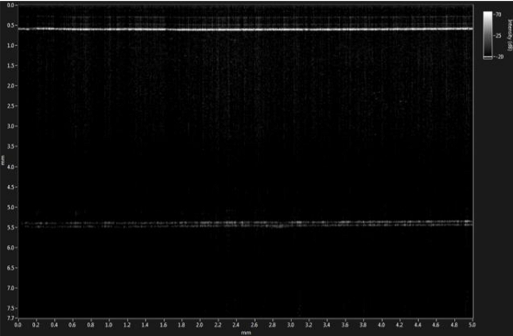
Fig. 10. OCT image of polymer used for printing. Lack of the scattering centers indicates no occurrence of the diamond nanoparticles.

“In this research we have shown that the presence of nanodiamond affects the optical characteristics of the mixture,” the researchers concluded. “It gives premises that other nanoparticles can modify the optical properties, especially absorption characteristics. Therefore, it may lead to new opportunities for a low-cost, quick and easy method for rapid prototyping of optical filters.”

Discuss this story and other 3D printing topics at 3DPrintBoard.com or share your thoughts in the Facebook comments below. 

The post New 3D Printing Resin Made with Nanodiamond Powder appeared first on 3DPrint.com | The Voice of 3D Printing / Additive Manufacturing.

What is Metrology Part 23 – Error and Perception

Margin of Error

After a significant amount of time dedicated to this series, I have made some interesting insights.  When you think of metrology and measurement, humans need to understand that we are faulty at what we do. It is difficult to have true precision in measurement. We are prone to error and degrees of various errors. Secondly, no one human has the same perception as another. This leads to various incongruities in the physical realm. We can think in terms of optics, general psychology, and a vast number of phenomena. So how do we escape faulty perception and human error? Well, that seems impossible, but I am going to venture into these topics to show how they affect measurement and metrology as a whole.

Margin of error is a statistic that shows the amount of sampling error due to random occurrences. When we have a large margin of error, there lies less confidence in the data we collect. In reference to metrology, one can think of a scanning system as our measuring apparatus. When operated by a human, various things and random occurrences can affect the margin of error within a laser scan. This can include an unsteady hand when scanning an item. One could also have a slightly unclean lens that may cause distortion within a 3D scan. The movement of a target for 3D scanning may also affect this as well. There are a slew of items that may cause a 3D scan to contain large margins of error.

Act of Perception

Perception is how we organize, identify, and interpret sensory information in order to understand or represent our environment. Perception includes the ability for us to receive signals that go through our nervous system. This results in physical or chemical stimulation of our sensory systems. This allows us to interpret and understand the information we are bombarded with on a daily basis. Examples of this include how vision occurs through light interacting with our eyes, how we are able to use odor molecules to interpret smell, as well as our general ability to detect sound through pressure waves within the air. Perception is denoted by the receiver though. This means their learning, memory, expectation, and attention are vital for how the signals are interpreted.

I bring these things up as it shines a light on a key difference between machines and humans. Machines have less working experience, expectation, and learning compared to humans. Being able to consistently distinguish a watch in 3D form is natural for most humans, but a machine can be thrown off by slight variations in form. A machine automated process may have less error in terms of pure measurement, but the interpretation of the data is still a difficult task for a machine.

Issues of Perception and Metrology

Perception is typically thought of in two forms:

  • Processing an input that transforms into information such as shapes within the field of object recognition.
  • Processing that is interloped with an individual and their own concepts or knowledge. This includes various mechanisms that influence one’s perception such as attention.

Through laser scanning, an individual is able to collect data on a physical product. This data needs interpretation for it to have tangible value. A computer device is not readily able to do so. So metrology is a field based on our innate error and psychology as humans. But that does not mean the field is useless, as we humans have an innate desire to make things quantifiable.

The post What is Metrology Part 23 – Error and Perception appeared first on 3DPrint.com | The Voice of 3D Printing / Additive Manufacturing.

Optical Machine Learning with Diffractive Deep Neural Networks #MachineLearning #3Dprinting #DeepLearning #NeuralNetworks #TensorFlow @InnovateUCLA

From techxplore.com. Credit: UCLA Engineering Institute for Technology Advancement


The Ozcan Lab at UCLA has created optical neural networks using 3D printing and lithography. TensorFlow models were trained on the MNIST, Fashion-MNIST, and CIFAR-10 data sets using beefy GPUs. The trained models were then translated into multiple diffractive layers. These layers create the optical neural network. What the model lacks in adaptability it gains in speed as it can make predictions “at the speed of light” without any power. The basic workflow involves passing light through an input object which is filtered through the entire optical neural network to a detector which captures the results.

…each network is physically fabricated, using for example 3-D printing or lithography, to engineer the trained network model into matter. This 3-D structure of engineered matter is composed of transmissive and/or reflective surfaces that altogether perform machine learning tasks through light-matter interaction and optical diffraction, at the speed of light, and without the need for any power, except for the light that illuminates the input object. This is especially significant for recognizing target objects much faster and with significantly less power compared to standard computer based machine learning systems, and might provide major advantages for autonomous vehicles and various defense related applications, among others.

If you’d like to learn more about Photonics checkout the research happening at the Ozcan Lab. If you’d like more details about diffractive deep neural networks checkout this publication in Science or the most recent Ozcan Lab publication on the topic.

What is Metrology Part 2: CMM

Image result for cmm

CMM

A CMM is a widely used machine used to measure objects. A CMM is a coordinate measuring machine. This refers to any machine that measures the geometry of physical objects by sensing discrete points on the surface of the object with a probe. This is the essence of many a metrology system. The precision of a CMM is vital for determining the geometry of objects. This then leads to more precision in the manufacturing and replication of objects. 

Probes are the engine of a CMM. They sense objects through their surfaces. There are various types of probes as well.  The types of probes used in CMMs include mechanical, optical, laser, and white light. Mechanical probes typically have a ball and rod looking setup attached to them, or have a nozzle setup. These physically touch the surface of a material that is in need of measuring. Optical probes typically refer to spectral analysis and measuring through these means. One can think of a fiber optic probe in particular. These type of probes are usually used in Raman spectroscopy, and diffuse reflection applications. Raman spectroscopy is a spectroscopic technique based on inelastic scattering of monochromatic light, usually from a laser source. Inelastic scattering means that the frequency of photons in monochromatic light changes upon interaction with a sample. The scattering of the photons within a monochromatic light source allows for a device to detect if an object is within the path of monochromatic light. This thus leads to measuring capabilities that are important in terms of a CMM as well. Diffuse reflection is similar to Raman Spectroscopy aside from the optical source is typically infrared. When an IR beam passes through a physical object, it can be reflected off the surface of a particle or be transmitted through a particle. The IR energy reflecting off the surface is typically lost. This transmission‐reflectance event can occur many times in the object, which increases the pathlength. This pathlength is vital for measuring. Finally, the scattered IR energy is collected by a spherical mirror that is focused onto the detector. The detected IR light is partially absorbed by particles of the object, collating the object information.

Image result for raman spectroscopy

Typical Raman Spectroscopy Setup

A CMM is heavily reliant on a built-in coordinate system of, typically, three axes. This is similar to the coordinate systems we are aware of within a 3D build environment. This is a Cartesian Coordinate system. The main structure of which includes three axes of motion. The material used to construct the moving frame has varied over the years. Granite and steel were used in the early CMM ‘s. Today the major CMM manufacturers tend to build frames from aluminium alloy or some derivative and also use ceramic to increase the stiffness of the Z axis for scanning applications. CMM axises need to be stiff because there should be minimal outside inference with forces that may misalign the device during measurement. Any misalignment will cause higher error ranges for measurement. 

Image result for cartesian coordinate system

Cartesian Coordinate System

Scanning techniques are becoming more reliant on data collection and compilation. These methods use either laser beams or white light that are projected against the surface of a part. Thousands of points can then be taken and used not only to check size and position but also to create a 3D image of the part also. This “point-cloud data” can then be transferred to CAD software to create a working 3D model of the part. The ability to hold various point cloud data from these methods is essential for the future development of the field. Big data is something of interest most definitely for this field. 

CMM’s are very interesting and are the basis of most metrology methods. It is important to understand how in-depth and fascinating this field is. It is a very vital one as well for the future in terms of 3D printing and manufacturing. Stay tuned for the next installment where we take a look into different subfields within Metrology as well.

The post What is Metrology Part 2: CMM appeared first on 3DPrint.com | The Voice of 3D Printing / Additive Manufacturing.

Nanofabrica Releases Micron Resolution 3D Printing Platform Aimed at Industrial Applications

Israeli 3D printing startup Nanofabrica, which was founded in 2016 and chosen by the the I-YBI collaborative in 2017 to get help entering the American market, is working to mass-produce 3D printed parts on the micro and nanoscale. Now, its hard work has paid off, as the company just commercially launched, in the words of CEO Jon Donner, a true “mass manufacturing” micron resolution that’s targeted directly at pan-industrial micro manufacturing applications expanding throughout sectors like aerospace, automotive, medical, optics, and semiconductor.

Most manufacturers looking to fabricate tiny components and product in volume, with features at the micron resolution, have had to use more traditional micro molding and machining technologies. But the startup’s micro 3D printing process is cost-effective and fast, with the ability to achieve highly accurate results.

“The discipline of Additive Manufacturing (AM) or 3D Printing (3DP) is regularly cited as being disruptive to traditional manufacturing processes,” Donner wrote.

“AM has made the shift from a prototyping technology to a true production technology, but many lack the insight about what can really be produced on AM platforms, and the inherent characteristics of the process that add significant advantages when it come to cost, complexity, and timeliness of manufacture.”

3D printer manufacturers are doing what they can to combat adoption barriers, and are refining their technologies by adding valuable features or looking for niches that are under-served, or not even served at all…such as micro manufacturing.

“When viewed from the perspective that across industry today there is an inexorable shift towards miniaturisation, with many applications demanding extremely exacting levels of micron and sub-micron precision on macro and micro parts, there is huge potential for an AM platform that can service this trend,” Donner stated. “A whole raft of traditional production platforms have developed to cater for this demand, but until recently, the ability for AM to produce such precision at all —let alone at volume production levels — has been impossible.”

Nanofabrica develops its own proprietary materials, focusing on common plastics like ABS and PP. Its AM platform is perfectly tailored for micro and nano manufacturing, and, according to TCT, is made up of two new 3D printers: the Industrial System, said to achieve a one-micron resolution with a 50 x 50 x 100 mm build volume, and the Workshop system. This provides manufacturers who need “micron and sub-micron levels of resolution and surface finish” with a bespoke end-to-end solution.

“Successful AM platform developers in today’s crowded market need to focus technological advances on areas that open up innovation and the manufacture of products and components hitherto impossible using AM,” Donner wrote. “It is here that Nanofabrica has been particularly successful, having identified a series of killer applications where there is burgeoning market demand, where the only route to market at the moment is through disproportionately expensive or restrictive traditional manufacturing technologies, and where the use of AM can open up significant advances on terms of design and functionality.

“These killer applications exist in the area of optics, semi-conductors, micro electronics, MEMS, micro fluidics, and life sciences. Products such as casing for microelectronics, micro springs, micro actuators and micro sensors, and numerous medical applications such as micro valves, micro syringes, and micro implantable or surgical devices.”

Nanofabrica’s new 3D printers are based on a Digital Light Processor (DLP) engine, which is combined with adaptive optics to ensure repeatable micron levels of resolution – a necessary feature when creating cost-effective, highly precise components for industrial manufacturing. Additionally, the AM platform uses multiple sensors to allow for a closed feedback loop, which also helps deliver high accuracy.

The startup’s AM platform is also unique in how it combines several technologies in order to “achieve micron resolution over centimeter-sized parts.”

Donner explained, “Specifically, the company has taken its innovative use of adaptive optics and enhanced this imaging unit with technology and know-how used in the semiconductor industry (where the attainment of micron and sub-micron resolutions over many centimetres is routine.) By working at the intersection of semiconductors and AM, Nanofabrica is able to build large “macro” parts with intricate micro details. It can also do this at speed by introducing a multi resolution strategy, meaning that the parts where fine details are required are printed relatively slowly, but in the areas where the details aren’t so exacting, the part is printed at a speeds 10 to 100 times faster. This makes the entire printing speed anything from 5 to 100 times faster than other micro AM platforms.”

Nanofabrica’s hardware enables multi resolution capability due to “a trade off between speed and resolution,” while its software algorithms define and section off both the part and its 3D printing path into low and high resolution areas to be fed into the machine parameters and path. A “spectrum of resolutions” make it possible to optimize speed and achieve “satisfactory results,” while the “final algorithm family” is focused on file preparation and optimizing parameters like supports and print angle.

“Perhaps of key interest is the fact that AM is relatively agnostic to part complexity, and it is possible to design and manufacture unique geometries. As such, the Nanofabrica technology becomes an enabling technology, and a true stimulator of innovation, making the manufacture of parts and features previously impossible, possible,” Donner said.

“Nanofabrica is aware — as the first mover in the micro AM space for production — that it establishes a partnership relationship with its customers that extends from product inception through to mass manufacturing. The technology is today the only micron-resolution platform aimed at true manufacturing applications not just R&D projects, the real game changer being the combination of commercially-oriented build volumes, optimised materials, significant lines of investment, and a platform that is competitively priced.”

The startup is also an advocate of customer collaboration for the purposes of optimizing outcomes, and provides advice on design for additive manufacturing (DfAM), which is often used for macro AM platforms but not micro.

“It is because of this that Nanofabrica promotes a collaborative relationship with its customers to locate the opportunities and avoid the bear traps that exist when adopting — or considering adopting — AM for production purposes in the micro manufacturing arena,” Donner said.

Nanofabrica’s micro 3D printing platform is still new, which is another reason it’s looking to ” partner with key players in relevant sectors.” This will allow the startup to better customize its technology for specific applications in a variety of markets.

Discuss this and other 3D printing topics at 3DPrintBoard.com or share your thoughts below.

[Images provided by Nanofabrica]