Wear-Resistant Tungsten 3D Printer Nozzle Launched on Kickstarter

Just a few months ago, we learned from 3D°Hex that it would soon be launching a Kickstarter campaign for a new, highly temperature and wear resistant tungsten 3D printing nozzle, called the Tungzzle, that it had been working to develop for about a year. The startup, based in the Ruhr region of western Germany, is focused on designing and manufacturing better 3D printing materials and components in order to solve some of the current problems in the 3D printing industry, and started with the Tungzzle, which, as you may guess from its name, is made of an alloy with 95% pure tungsten content, and not a combination.

We’ve just learned from 3D°Hex that the crowdfunding campaign for its Tungzzle is now live on Kickstarter.

“The most affordable wear and high temperature resistant 3D-Printing nozzle on the market, made completely of tungsten heavy alloy,” the 3D Printing Tungsten Nozzle campaign’s headline claims. “While many new, cutting-edge 3D-Printing nozzles hit the market every few months, there is a huge disparity in their respective qualities. If you want something that is reliable and durable, you need to put some effort into selecting the right technology.  You want something that is affordable, of course, but you want also something reliable, that will produce high quality as well.”

The nozzle is the last piece of your machine that touches your print, so it’s important that it can perform reliably. 3D°Hex founders Christopher and Paul explain on the Kickstarter campaign page that when you need an individual printer nozzle for specific tasks, you may be shelling out a high amount of money for something you’ll be using on a lower cost desktop printer. But they say that the Tungzzle combines all the important benefits of these different nozzles into one. This allows the startup to, as it told us in April, create “the ultimate balance between performance and price.”

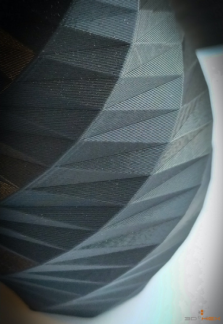
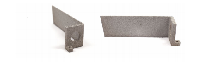
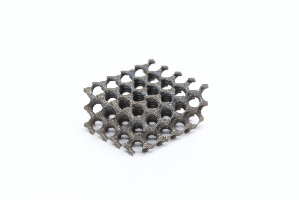
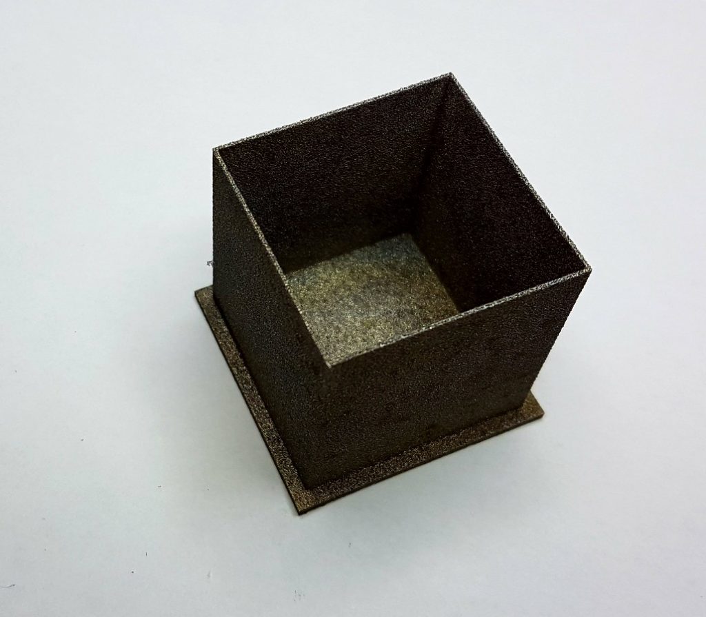
3D printed part made of carbon fiber-reinforced filament, printed using the 3D°Hex Tungzzle.

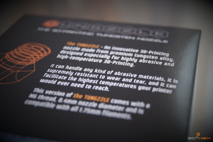
Tungsten is an extremely dense (19.3 g / cm3) and hard (7.5 up to 8 on Mohs scale) metal, with high wear resistance and thermal conductivity, and features the highest critical melting point of all refractory metals. All of these properties mean that the Tungzzle, which is made of 95 WNiFe Tungsten heavy alloy, can print with highly abrasive materials, like carbon fiber, without the inside of the nozzle being damaged, and that it can also work with high temperature materials such as PEEK and nylon. Its excellent thermal conductivity allows for better extrusion performance out of your printer, in addition to better temperature calibration effects.

“With steel with a coefficient of 10.8 to 12.5 and brass with a coefficient of 18 to 19, tungsten has one of the lowest expansion coefficients with 4.5 and does not experience an extreme tempering effect, which means that its properties are retained even at long high-pressure temperatures,” the Kickstarter campaign states.

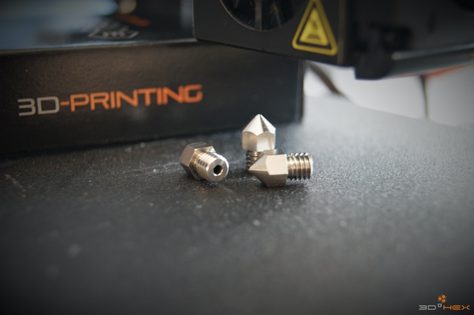
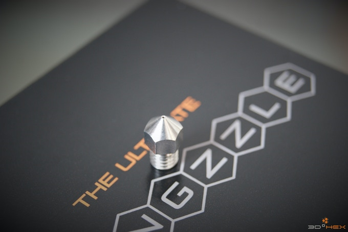
The Kickstarter campaign has plenty of available rewards left, such as the €12 Supporter pack, which comes with a Tungzzle sticker set and a carbon fiber 3D printed 3D°Hex logo, and the €15 3D°Hex supporter t-shirt. The Ultimate Tungzzle Super Early Bird reward is just €29, which saves 55% off the RRP and comes with the Tungzzle itself, which features an M6 thread, 0.4 diameter, and works with 1.75 mm FDM 3D printing filament. A double Tungzzle pack is €74, while a triple pack is €107, and you can purchase a pack of five Tungzzle 3D printer nozzles for €160.

(Images courtesy of 3D°Hex)

The post Wear-Resistant Tungsten 3D Printer Nozzle Launched on Kickstarter appeared first on 3DPrint.com | The Voice of 3D Printing / Additive Manufacturing.

NASA Seeks Proposals to Advance AM Techniques for High Temperature Materials

The National Aeronautics and Space Administration (NASA) is seeking proposals from university research teams to develop unique, disruptive, and transformational space technologies that are currently at low technology readiness levels (TRL) but have the potential to lead to dramatic improvements at the system level. One of the topics of the Space Technology Research Grants (STRG) Program, Early Stage Innovations (ESI) appendix focuses on the advancement of additive manufacturing (AM) processing techniques for high-temperature materials.

Supporting education and research is a great way to advance the space exploration capabilities of NASA. In fact, according to the space agency, investment in innovative low-TRL research increases knowledge and capabilities in response to new questions and requirements; stimulates innovation, and allows more creative solutions to problems constrained by schedule and budget. Further suggesting that investment in fundamental research activities has historically benefited the United States by generating new industries and spin-off applications.

As an extension of the Space Technology Mission Directorate (STMD), the STRG Program is fostering the development of innovative, low-TRL technologies for advanced space systems. The goal of this particular endeavor is to accelerate the development of groundbreaking, high-risk but high-payoff, space technologies. It is not necessarily directed at a specific mission, but instead will support the future space exploration and science needs of NASA, other government agencies, and the commercial space sector; especially as plans for space colonization, lunar exploration, and future journeys to Mars advance.

Universities help drive many NASA projects today, researching everything from cube sat 3D printing to aerospace high-volume manufacturing. This new NASA solicitation is only for accredited US university proposals, and the research teams that apply for the STRG program can choose to focus on the advancement of AM processing techniques to improve properties of high-temperature refractory metals, particularly tungsten and tungsten alloys, as well as other refractory metals and alloys.

Deep space exploration mission prep (Credit: NASA)

As described by the agency, all the submitted proposals working on additive manufacturing processing techniques for refractory metals should address at least one of the following research areas:

  • Improving high-temperature material properties,
  • Improving surface roughness from the AM process to minimize future post-processing needs,
  • Altering surface characteristics to tailor emissivity and wetting properties (for example, to make them either hydrophobic or hydrophilic),
  • Developing AM techniques to eliminate/minimize porosity and microcracking of AM parts,
  • Developing post-processing techniques to eliminate/minimize the porosity and microcracking of AM parts,
  • Developing techniques and processes to improve the grain structure of AM refractory metals,
  • Developing AM techniques capable of fabricating with multiple metals at once, one of which is a refractory metal or alloy,
  • Developing refractory alloys that provide optimal properties for parts fabricated by AM methods.

Due to their high melting points and density, refractory metals and alloys are capable of operating at extreme temperatures and have become the frontrunners for many high-temperature aerospace components, as well as other high-temperature applications, such as nuclear reactors, electric furnaces, and welding.

Of all the metals in pure form, tungsten has the highest melting point of 6,192°F (3,422°C) and is often alloyed with other metals for strength. As some of the toughest materials found in nature, refractory metals could be ideal for spacecraft applications that have to endure severe heat during space travel. Space shuttles, for example, used to face intense temperatures when re-entering the Earth’s atmosphere, as high as 3000°F (1649°C). If space adventurers expect to travel to Mars and beyond, spacecraft need to be protected, and this early-stage research could determine the bases for the future development of protection needed for safe space journeys.

The aerospace industry is increasingly turning to AM for thermal management systems that are capable of operating at extreme temperatures. The agency proposed integrated thermal management systems as one example where additive manufacturing plays a fundamental role in enabling technology. High-temperature thermal management systems are potentially disruptive to a wide range of high-temperature NASA applications such as wing leading-edge systems, solar probes, and Nuclear Thermal Propulsion (NTP); and can benefit from improvements in the fabrication of refractory metal casing materials.

During this early stage research, NASA is solely focused on manufacturing under Earth’s gravity, and there is still no mention of demonstrating additive manufacturing capabilities in space. However, we can probably expect that as this research moves forward, zero gravity fabrication will be of interest.

European Space Agency astronaut Luca Parmitano tests experiments in space (Credit: NASA)

With a maximum award of $650,000 for a research period of three years or less, this research grant represents a great opportunity for academics focusing on AM processing techniques.

NASA considers that these investments create, fortify, and nurture the talent base of highly skilled engineers, scientists, and technologists to improve the country’s technological and economic competitiveness. The ESI Appendix challenges universities to examine the theoretical feasibility of new ideas and approaches that are critical to making science, space travel, and exploration more effective, affordable, and sustainable.

Historically black colleges and universities along with other minority-serving institutions are encouraged to submit proposals. Moreover, NASA encourages submission of ESI proposals by women, members of underrepresented minority groups, persons with disabilities, and faculty members who are early in their career.

As NASA seeks to develop unique, disruptive, and transformational space technologies, university researchers get a chance to participate in the next generation of space exploration efforts, that are a complement to many of the agency’s ongoing programs. The solicitation is available here and universities have time until May 20, 2020, to present their notice of intent, and until June 17, 2020, for proposals.

The post NASA Seeks Proposals to Advance AM Techniques for High Temperature Materials appeared first on 3DPrint.com | The Voice of 3D Printing / Additive Manufacturing.

University of Sheffield: Comparative Research of SLM & EBM Additive Manufacturing with Tungsten

Jonathan Wright recently submitted a thesis to the Department of Materials Science and Engineering at The University of Sheffield, exploring 3D printing with tungsten, a rare metal. In ‘Additive Manufacturing of Tungsten via Selective Laser Melting and Electron Beam Melting,’ Wright details the potential for powder bed additive layer manufacturing (ALM) of pure tungsten, using both selective laser melting (SLM) and electron beam melting (EBM).

Referring to the layered approach of 3D printing or additive manufacturing, Wright chooses to encompass most of this technology as ALM, reminding us that Chuck Hull of 3D Systems fame was granted the patent in 1986 after he created stereolithography (SLA).

Schematic Diagram of the SLA Process. Diagram taken from ’Apparatus for production of three-dimensional objects by Stereolithography’
Patent application [1]

“An advantage of the ALM approach is the fact that no additional tooling is required for new components,” stated Wright. “This tool-less approach results in shorter lead times and reduced cost for new products.”

Users in a variety of industries today also enjoy major benefits such as less waste in material, greater savings on the bottom line, and the potential for environmentally friendly processes in some cases, whether powder-based, liquid-based, or solid deposition.

An overview of ALM processes and hardware (adapted from [6])

Tungsten, derived from wolframite ((Fe,Mn)WO4) and scheelite (CaWO4), not only has the lowest vapor pressure of any element but also offers a high melting point and the capability for being ‘drawn into fine wire.’ Used in lamp filaments and a variety of other applications today, it can be used in high temperatures or in cases where high density is required such as X-ray shielding.

Wright also explains that because of tungsten’s thermal properties, ‘low spluttering yield, and short activation decay time,’ it is also suitable for nuclear fusion experiments.

“Tungsten can be machined, (drilled, turned, milled, etc.) however this is difficult, requires expertise, and close adherence to ideal conditions,” states Wright. “Structures with greater complexity can be formed by Electrical Discharge Machining (EDM) overcoming some of these difficulties.”

Because there are challenges and limitations due to the chemical, physical, and mechanical makeup of tungsten, alloying is a consideration; however, Wright notes that a ‘huge number’ of alloys have been examined but not found to be important. So far, tungsten-rhenium alloys have been considered to show the greatest potential for improving ductility.

A general flow diagram for the hydrometallurgy of tungsten [62]

During the experimental phase of Wright’s study, he used a Renishaw SLM 125 to fabricate sample parts, as well as a Renishaw AM 400 for other builds.

Renishaw SLM 125 System

For EBM processes, an Arcam S12 system was used.

Schematic of ARCAM S12 EBM System. Image from arcam.com

Wright discovered that it was not possible to create tungsten parts without defects, and that beam power was one of the greatest reasons for porosity, with all samples exhibiting high levels at 200W and for 400W, the lowest.

“As porosity in tungsten samples produced via SLM was reduced the number of cracks was found to increase, this was also therefore a function of beam power,” explained Wright.

“Further work needs to be carried out on SLM of tungsten in order produce crack free parts. This may include an investigation of adding an external heat source. A heated environment is likely to reduce residual stresses and raise material above the DBTT.”

A tungsten Langmuir Probe manufactured via SLM. 25mm in length

In experimenting with fabrication of EBM samples, Wright was able to pinpoint the proper parameters for tungsten samples with low defects. He identified speed, current, and hatch spacing as playing a large role in porosity.

A tungsten mono-block manufactured via EBM. External dimensions
of 20mm x 20mm x 25mm

A tungsten lattice structure manufactured via EBM. External diameter:
80mm. Thickness 20mm

“For the first time EBM of tungsten has been reported. Specifically, EBM was able to produce low porosity, crack free parts. EBM appears to the preferable manufacturing process due to its combination of a vacuum environment, high build temperatures and high beam power,” concluded Wright.

“Nonetheless, mechanical properties and geometric accuracy require further improvements before ALM can be used to manufacture tungsten for structural applications. For Applications where mechanical properties are non-critical and complex geometry is required, such as in x-ray collimation, the ALM techniques outlined here could provide a viable processing route.”

As researchers around the world continue to refine 3D printing and AM processes, tungsten is being investigated from examining its properties, to fabricating cutting tools, and large unalloyed parts.

What do you think of this news? Let us know your thoughts! Join the discussion of this and other 3D printing topics at 3DPrintBoard.com.

[Source / Images: ‘Additive Manufacturing of Tungsten via Selective Laser Melting and Electron Beam Melting’]

The post University of Sheffield: Comparative Research of SLM & EBM Additive Manufacturing with Tungsten appeared first on 3DPrint.com | The Voice of 3D Printing / Additive Manufacturing.

Fraunhofer ILT: Making Tungsten Carbide-Cobalt Cutting Tools with LPBF 3D Printing

Obviously, the Fraunhofer Institute for Laser Technology ILT does a lot of work with lasers, and, in the same vein, with metal 3D printing processes that use lasers. Now, it’s teaming up with scientists from the Institute for Materials Applications in Mechanical Engineering IWM and the Laboratory for Machine Tools and Production Engineering WZL, both at RWTH Aachen University, to investigate laser processes for the 3D printing of cutting tools made of tungsten carbide-cobalt (WC-Co).

The new AiF project – “Additive Manufacturing of Machining Tools out of WC-Co – AM of WC-Co” – began on October 1st 2019 and will last for 30 months; funding is provided by the Otto von Guericke e.V. working group of industrial research associations.

Cutting tools made of WC-Co are very heat- and wear-resistant, which is what one generally wants in this type of application, but it’s not easy to use conventional methods of manufacturing to create them. Complex sintering processes are currently used, but it’s not ideal, as only a restricted amount of geometrical freedom is possible, and it’s expensive and difficult to introduce complex cooling structures into the tools as well.

The process development aims to generate a homogeneous, almost dense structure of the WC-Co-composite, as shown here in this SEM measurement. [Image: Institute for Materials Applications in Mechanical Engineering IWM, RWTH Aachen University]

One of the project goals is to create cutting tools with integrated complex cooling geometries in order to ensure longer tool life. That’s why the Aachen researchers are looking into Laser Powder Bed Fusion (LPBF) 3D printing for WC-Co cutting tool fabrication, which offers near-net-shape production for generation of cooling structures within these tools, and far more design freedom. This technology requires users to carefully choose their process and material parameters in order to create components with strength that’s comparable to what could be achieved with conventional manufacturing methods.

For the past few years, Fraunhofer ILT scientists have been researching a major problem in the LPBF process – temperature distribution in the part. Conventional systems slow down the cooling process with a heated base plate, but with LPBF, the metal powder is melted where the laser touches it and cools down quickly, which can cause cracks and tension.

Fraunhofer ILT has been working with adphos Innovative Technologies GmbH on this issue, and together the two created a system which uses a near-infrared (NIR) emitter to heat the component from above to over 800°C. This system is what Fraunhofer ILT and its fellow Aachen researchers are using to process tungsten carbide-cobalt material for cutting tools in the “AM of WC-Co” project.

Under the scope of the project, the researchers are investigating the process route all the way from powder formation and 3D printing to post-processing and testing the components. Together, they will qualify the materials and processes that will replace complex sintering processes in fabricating these cutting tools.

Preheating the machining plane with the NIR module significantly reduces stresses in the laser-manufactured component. [Image: Fraunhofer ILT]

3D printed WC-Co cutting tools will have a hardness comparable to those made with conventional manufacturing methods, but because of the cooling structures that the LPBF process can be used to create, they will have a longer service life. Additionally, the NIR emitter system developed by Fraunhofer ILT and adphos can lay the groundwork for processing refractory alloy systems in the future.

At formnext 2019, in Frankfurt from November 19-22, you can stop by the Fraunhofer Additive Manufacturing Alliance booth D51 in Hall 11 to learn more about the collaborative “AM of Wc-CO” project.

Discuss this story and other 3D printing topics at 3DPrintBoard.com or share your thoughts in the Facebook comments below. 

[Source: Fraunhofer ILT]

The post Fraunhofer ILT: Making Tungsten Carbide-Cobalt Cutting Tools with LPBF 3D Printing appeared first on 3DPrint.com | The Voice of 3D Printing / Additive Manufacturing.

Cranfield University Researchers Use WAAM Process to Produce Large-Scale Parts in Unalloyed Tungsten

Large-scale unalloyed tungsten linear structure deposited via WAAM (a-b). Picture of the fracture from the outer surface (c) and SEM picture of the fractured surface (d).

Cranfield University is continuing its work with Wire and arc additive manufacturing, or WAAM: a novel process that uses an electric arc as the heat source, and high-quality metal wire as the feedstock. A trio of researchers with the university’s Welding Engineering and Laser Processing Centre (WELPC) published a paper, titled “Development of Wire + Arc Additive Manufacturing for the production of large-scale unalloyed tungsten components,” which demonstrates that WAAM can produce large-scale parts in unalloyed tungsten by complete fusion. This is a possible alternative to using powder metallurgy for manufacturing tungsten.

The abstract reads, “The manufacturing of refractory-metals components presents some limitations induced by the materials’ characteristic low-temperature brittleness and high susceptibility to oxidation. Powder metallurgy is typically the manufacturing process of choice. Recently, Wire + Arc Additive Manufacturing has proven capable to produce fully-dense large-scale metal parts at relatively low cost, by using high-quality wire as feedstock. In this study, this technique has been used for the production of large-scale tungsten linear structures. The orientation of the wire feeding has been studied and optimised to obtain defect-free tungsten deposits. In particular, front wire feeding eliminated the occurrence of pores and micro-cracks, when compared to side wire feeding. The microstructure, the occurrence of defects and their relationship with the deposition process have also been discussed. Despite the repetitive thermal cycles and the inherent brittleness of the material, the as-deposited structures were free from internal cracks and the layer dimensions were stable during the entire deposition process. This enabled the production of a relatively large-scale component, with the dimension of 210 x 75 x 12 mm.”

Microstructure of the linear structure deposited using front wire feeding (a). Details of elongated grains at the center of the structure (b, d). Detail of microstructure of the upper part (c) and base of the linear structure (e).

Tungsten is a major candidate for manufacturing components in the energy sector, which require materials with high heat resistance, neutron load-capacity, and excellent mechanical properties. Because tungsten has the highest melting point of all metals, along with low tritium retention, relatively high thermal conductivity and density, and good resistance to sputtering and erosion, it can be used in in future fusion reactors as a plasma-facing material. But, due to the metal’s high recrystallization temperature and low fracture toughness, it’s not that easy to manufacture tungsten components.

“Currently, there are three main manufacturing operations that are being studied, when referring to tungsten components for nuclear fusion environment: the industrial production of large-scale components; the joining of these parts with other materials; and their efficient repair and maintenance,” the researchers explained, noting that additive manufacturing can be used to manufacture the alloy.

“AM could definitely address some of the manufacturing issues related to tungsten components, and possibly enable the development of new designs approaches.”

WAAM is able to directly fabricate large, fully-dense, metallic, near-net-shape components at a higher deposition rate than other metal 3D printing processes. So the team wanted to apply WAAM for the first time to unalloyed tungsten, paying special attention to creating large-scale components that were free of defects.

“The study and monitoring of the metal transfer, and the characterisation from the microstructural point of view are discussed,” the researchers wrote. “A structure of realistic scale has also been produced to understand the issues related to scaling up, and ultimately assess the feasibility of WAAM’s implementation as an innovative way to produce unalloyed tungsten parts.”

Setup for development of WAAM process for unalloyed tungsten when using side wire (a) and front wire feeding (b).

The above image depicts the apparatus the team used for deposition. For the side wire and front wire feeding configurations, tungsten layers were deposited progressively onto the substrate, in a constant direction, with a single bead. The cross-section perpendicular to the direction of the deposition was ground up, polished, and etched, in order to examine defects and the microstructure. Once the researchers landed on the optimal parameters, they used the WAAM process to build a tungsten wall that was 120 mm in length, 75 mm high, and 12 mm thick.

Time-resolved images of the deposition performed using side wire feeding configuration.

While there were no signs of spatter during deposition for the front wire feeding, there were some spattered particles during the side wire feeding configuration, mainly caused by two main ejection mechanisms.

“The droplets or macroscopic mass losses, localised predominantly along the melted surface, arose because of the Kelvin–Helmholtz instability,” the researchers explained. “This phenomenon occurs when there is a difference in velocity across the interface between two fluids. Furthermore, it has been reported that the Kelvin–Helmholtz instability can also lead to the evolution of shock waves along the surface of the fluid causing a breakup of the melt surface into droplets.”

This lack of spattered particles on the front wire feeding directly correlates to a lack of fusion and pores in the structure, so it’s important to avoid spatters if you want to keep the WAAM-deposited tungsten structure strong.

With both side- and front-fed deposit, the microstructure contained fine equiaxed grains near the bottom layers, with larger, more coarse grains near the top. The team explained that the tungsten’s high thermal conductivity at room temperature, along with rapid solidification, promoted the equiaxed grains.

“This possibly represents the first fully-dense large-scale structure in unalloyed tungsten produced using AM. The unique aspects of this structure were the absence of any large network of grain boundary cracks within the volume deposited, the almost absence of discolouration and oxidation from the fusion process, and the consistency in the layers’ geometry,” the team stated.

Tungsten linear structure deposited using side wire feeding (a).

The study showed that, while WAAM technology can produce “large-scale refractory metal components by complete fusion” out of high-purity tungsten, the orientation of the wire feeding can majorly influence the deposit’s microstructure, along with creating structural defects and pores.

Co-authors of the paper are G. Marinelli, F. Martinaa, S. Gangulya, and S. Williams.

Discuss this and other 3D printing topics at 3DPrintBoard.com or share your thoughts below.

A Look at the Properties of 3D Printed Tungsten

Tungsten is a dense, robust metal that has a number of valuable applications, particularly in the chemical industry thanks to its corrosion resistance. Its hardness and extremely high melting point, however, have made it a difficult material to 3D print. In a paper entitled “Effect of processing parameters on the densification, microstructure and crystallographic texture during the laser powder bed fusion of pure tungsten,” a group of researchers addresses those challenges.

“This work looks to extend its [laser powder bed manufacturing’s] use to refractory metals, such as those considered in this paper where the behaviour of pure tungsten powder is investigated,” the researchers explain. “A strategy for fabricating high density parts was developed by creating a process map in which the effect of laser energy density was studied. The process quality was assessed using different techniques including light optical microscopy, XCT, SEM and EBSD. The results showed that the laser energy density was adequate to process tungsten to produce functional parts.”

Depending on the process conditions, the bulk density and optically determined densities of the tungsten ranged from 94 to 98%, but the parts showed micro cracks and defects due to micro- and macro-scale residual stress.

“Analysis of the microstructure and local crystallographic texture showed that the melt pool formed under the laser beam favoured solidification in a preferred orientation by an epitaxial growth mechanism,” the researchers continue. “The EBSD local texture analysis of the tungsten specimens showed a <111>//Z preferential fibre texture, parallel to the build direction.”

Two types of tungsten specimens were 3D printed, and were analyzed using scanning electron microscopy. Although the parts were prone to cracking, the researchers determined that the density and quality of the specimens produced in the 3D printing process were sufficiently high for use in applications such as medical radiation shielding and nuclear imaging, and in other plasma facing environments. They also concluded that the parameters for laser powder bed fusion could be tailored to fabricate tungsten parts with relatively high densities.

“Analysis of the microstructure, global and local crystallographic texture showed a columnar grain structure generated by an epitaxial re-growth mechanism, as noted in other AM processes with pure metals,” they add. “Using a laser energy density of up to 348 J/mm3 led to samples showing an unusual strong <111>//Z fibre texture. It is postulated this may be related to the deeper melt pool shape than normally seen in LPBF because of the high thermal conductivity and surface tension of tungsten, combined with the 67° raster direction rotation employed between deposited layers in the Renishaw AM machine.”

3D printing tungsten allows for new applications for the material, as it can produce parts with high levels of accuracy and complexity. Tungsten 3D printing has been studied before by other researchers, and 3D printed tungsten components have even been commercialized. Despite its challenges, tungsten has shown itself to be a valuable 3D printing material that many experts are excited about for its heat resistant properties in particular.

Authors of the paper include A.T. Sidambe, Y. Tian, P.B. Prangnell and P. Fox.

Discuss this and other 3D printing topics at 3DPrintBoard.com or share your thoughts below. 


Wolfmet 3D 3D Prints 100% Tungsten Using SLM Showcases Its Products at TCT Birmingham 2018

Wolfmet 3D is the commercialization of 3D Printing methods developed at M&I Metals to 3D print tungsten. The company is a service bureau that makes tungsten 3D printed components for industry. Tungsten is not completely new to 3D printing with us having written about a study looking into the parameters of 3D printed tungsten and looking at Philips subsidiary Smit Rontgen 3D printing tungsten.

Now, Wolfmet 3D will try to conquer the world with this very special very dense material that for our industry is very exotic. To introduce their product the Wolfmet3D team is exhibiting at the TCT show in Birmingham and we interviewed them about 3D printing tungsten. Curious about them? Check them out at stand G41.

What is Wolfmet 3D?

Wolfmet 3D is the revolutionary additive manufacturing process whereby we produce 3D printed parts via SLM. It allows us to make parts which would either be impossible or not economical using traditional subtractive techniques.

What are the applications for 3D printed tungsten?

Extensive! It really is a very exciting time. Medical and industrial imaging in many ways are at the forefront of recent developments, but we are making new advances all the time in other areas too. To give just one example, we are in discussions with clients interested in tungsten’s heat resistant properties, which opens up another field of possible applications.

Tungsten is a very heavy metal. We almost always think about lightweighting things using 3D printing. But your material is used to make things heavier?

As you indicate, tungsten has a very high density (approx. 60% denser than lead). In the applications we have discovered so far for Wolfmet 3D, it is valued for its radiation attenuation properties, derived from the density, and also its heat resistance. The weight is really incidental.

What do you see as future applications for 3D printing tungsten?

Future opportunities are perhaps only limited by our own imagination, so our specialists work in partnership with leading research institutes and universities to ensure we are at the forefront of new developments across the globe.

How is tungsten used in vibration damping?

Tungsten’s high density enables it to act as a vibration weight in various dynamic applications.

Why does one want to 3D print a collimator?

The collimator’s function in an imaging system is to focus beams of radiation (gamma or x-ray) onto a detector and to filter out stray beams which might distort the signal. The detector’s software converts the signals into a 3D image of the subject. Until the arrival of Wolfmet 3D, most collimators were made from lead. Lead has several disadvantages – it is toxic and has to be handled with care and it is relatively soft. Most importantly, from the point of view of imaging systems, its density is much lower than that of tungsten. As a result, lead collimators are much less effective in screening out stray beams and, therefore, give inferior image quality.

What is the DEPICT system?

The DEPICT system was developed by a consortium which included Kromek and the University of Liverpool. Its function is to measure the amount of radioactivity issuing from a thyroid cancer patient during radiation therapy. This enables the medical staff to personalise the dosage of each treatment according to the patient’s physique and metabolism. The DEPICT team acknowledged early on that a tungsten collimator would give much more accurate readings than a lead one and we are very proud to have worked with them on this project.

Do you see many more applications in MRI or imaging generally?

Yes absolutely, Wolfmet 3D helps to make the innovations of our clients possible. Wolfmet tungsten has been shown to be MRI compatible in terms of its magnetic properties. This, together with the advantages that using tungsten can bring, makes it an exciting prospect for the future.

Are imaging apertures also a good application for your technology?

“In principle, yes, if the design is complex, as is increasingly the case.”

Isn’t shrinkage a huge problem with tungsten?

There is no shrinkage with the SLM technology which we use. I believe that this is not always the case with other Additive Manufacturing methods.

What kind of part properties can you get with this material?

The density is typically 94 – 96%. We have a continuous improvement programme designed to optimise the physical properties.

What kind of alloys are available?

At present we offer 100% tungsten components but as this is such a rapidly developing market, we are of course looking at other options. We have clients who are interested in developing other tungsten-based materials, but I’m afraid that I am also prevented from saying more due to our confidentiality agreements.