
Researchers and engineers at Massachusetts Institute of Technology (MIT) are using 3D printing to develop soft, flexible brain electrodes using a conductive polymer liquid material. Carrying out research into the 3D printing of conducting polymers, MIT engineers are working on developing soft neural implants that conform to the brain’s contours and monitor activity over longer […]
Live Entrepreneurship & 3D Value Networks Sustainability and Concrete
3D Printing Pioneer Janne Kyttanen is doing a series about value networks. In an interview, Janne has explained to us what exactly this is. Subsequently, Janne kicked off the series with a video interview with BAM’s Jeroen Nuijten on 3D printing concrete. Now Janne will delve deeper into 3D printing concrete through a discussion with Robert Niven of Carboncure.
Essentially what Janne is trying to do is to in front of your very eyes evaluate a technology, learn and then hopefully establish a value network that disrupts this technology. Now Janne wants to delve deeper into one of the most common building substances in the world. Accused of much CO2 pollution is there such a thing as sustainability in concrete?
Janne thinks that now is the time to innovate in concrete.
“My second 3D value network chat revolves around sustainability. In this day an age, it is hard for companies to be successful unless this very word is tattooed on their forehead. The days are over where the decadent human can roam the planet without consequences. Some even say, the COVID pandemic is nature’s way of telling us to slow down. The air is purer all over the world now and turtles are laying more eggs on deserted beaches, which previously have been packed by people.”
“But this talk is not about turtles, but about sustainability in concrete, value networks and why they matter for the 3D printing industry. Before I give the stage for the experts, there is one basic takeaway I have learned from concrete and sustainability this year. Whilst there is bad rep in the news for concrete and how bad it is for the environment, the reason is, it is a gigantic industry. No matter what other gigantic industry you would put on the table as a comparison, they all create a level of “badness” for the planet. But if the benefits would not by far overrule the bad, they would simply disappear and that is for sure not happening for concrete.
However, it is no excuse why we could not do things better, which is why I have specifically invited Robert Nivem, CEO of Carboncure for my next talk. Let’s hear from him how their technology is reversing the CO2 emissions from concrete for the benefit of the entire industry and the world.”
The post Live Entrepreneurship & 3D Value Networks Sustainability and Concrete appeared first on 3DPrint.com | The Voice of 3D Printing / Additive Manufacturing.
PLA: The Effects of Annealing & Autoclaving on Mechanical Behavior of Desktop FDM Parts
Researchers from the University of California delve into a very important area of 3D printing for the medical field, experimenting with how sterilization processes affect materials. They released their findings in the recently published ‘Identifying a commercially-available 3D printing process that minimizes model distortion after annealing and autoclaving and the effect of steam sterilization on mechanical strength.’
3D printed models are currently changing the face of medicine in terms of patient-specific treatment, allowing for better diagnosis, education for patients and their families (and medical students), along with acting as pre-planning tools and surgical guides.
In relation to FDM 3D printing in medicine, the authors refer back to previous studies concluding that PLA was weakened by sterilization yet strengthened in annealing, explaining that the next viable step would be to find a 3D printing material that can withstand heat treatment and steam sterilization.
The team fabricated four 30 mm cubes as samples for the study, each featuring different infill—designed in Tinkercad and then 3D printed on a LulzBot Mini 3D printer.
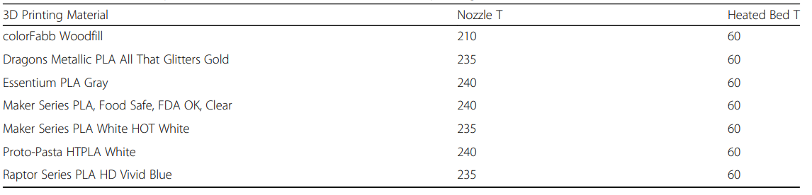
Manufacturer temperature (°C) recommendations for FDM 3D printing materials
Samples were printed all at once, using 0.38 mm layer height and a 0.5 mm printhead nozzle. Materials tested included:
- ColorFabb Woodfill
- Dragons Metallic PLA in All That Glitters Gold
- Essentium PLA in Gray
- Maker Series PLA in Food Safe FDA OK Clear
- Maker Series PLA in White HOT White
- Proto-Pasta HTPLA in White
- Raptor Series PLA in HD Vivid Blue
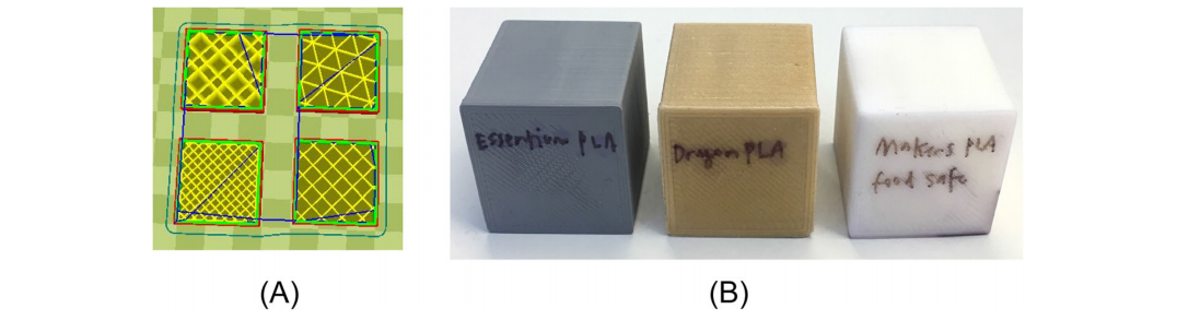
a) Infill geometries clockwise beginning from top-left: tetrahedral, triangles, grid, zig-zag and b) 3D printed cubes
Each sample was bathed in hot water, with the annealing treatment performed via an 800 W Strata Home sous vide circulating precision cooker.
“The cubes were removed from the hot water-bath and allowed to cool to room temperature without interference. The X, Y, and Z dimensions of the cubes were measured again to quantify deformation and calculate percent changes, a positive percent change indicating expansion and a negative percent change indicating shrinkage,” explained the researchers.
“In order to quantify distortion in either direction, we took the absolute value of these percentages. Subjective observations were noted such as spherical ‘balloon-like’ expansion. We also analyzed whether certain materials consistently expanded or contracted in every axes.”
Samples were then placed in autoclave sterilization pouches and deposited into a Tuttnauer 2540 M autoclave for 45 minutes at 134 °C and a pressure of 375 PSI. Afterward, the samples were cooled to room temperature and then examined for any signs of deformation.

a) Standard Army-Navy retractor and b) strength-optimized Army-Navy retractor designs in inches created in AutoDesk Fusion 360 obtained from Chen et al. c Retractor orientation on the build plate to eliminate need for support material
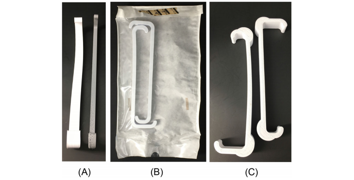
a) Standard retractors warping after hot water-bath annealing and b) after autoclaving. c) Strength-optimized retractor without intervention (right) and warping after hot water-bath annealing (left)
The material exhibiting the least amount of deformation was Essentium PLA Gray. The highest deformation was noted in Maker Series PLA White HOT White.

Quantifying absolute deformation in 30 mm cubes across 3D printing materials after annealing
“After hot water-bath annealing for 30 mm cubes, the infill that deformed the least was ‘grid,’ and the infill pattern that deformed the most was ‘zig-zag.’ After both annealing then autoclaving for 30 mm cubes, the material that deformed the least was Essentium PLA Gray. The material that deformed the most was Maker Series PLA White HOT White. After both annealing then autoclaving for 30 mm cubes, the infill pattern that deformed the least was ‘grid,’ and the infill pattern that deformed the most was ‘tetrahedral.’”
Quantifying absolute deformation in 30 mm cubes across 3D printing materials after annealing then autoclaving
Quantifying absolute deformation in 30 mm cubes across infill geometries after annealing then autoclaving
Maker Series PLA White HOT White was the only material noted to expand in every axis—despite the infill geometry or intervention. Every other material showed variances due to infill. Expansion after annealing usually seemed to suggest ‘direction of distortion’ after autoclaving.
“We acknowledge that dimensional changes and strength limitations may not be a challenge at a lower autoclave cycle, which would require further testing. We have also yet to understand the mechanical behavior of the 3D printed models in this study when they are subjected to multiple cycles of autoclaving and whether they will continue to undergo dimensional change. However, regardless of whether 3D printed PLA surgical instruments are determined to be single or multi-use, these instruments may still be valuable in fields such as aerospace medicine where space limitations exist, or in resource-limited situations where additional instruments are needed,” stated the researchers.
“This study is intended as a pre-clinical evaluation of the mechanical behavior of FDM 3D printing materials following hot water-bath annealing treatment and autoclave sterilization. For FDM 3D printed Army-Navy retractors, further sterilization and biocompatibility validation will be necessary for it to be applied clinically.”
What do you think of this news? Let us know your thoughts! Join the discussion of this and other 3D printing topics at 3DPrintBoard.com.
[Source / Images: ‘Identifying a commercially-available 3D printing process that minimizes model distortion after annealing and autoclaving and the effect of steam sterilization on mechanical strength’]
The post PLA: The Effects of Annealing & Autoclaving on Mechanical Behavior of Desktop FDM Parts appeared first on 3DPrint.com | The Voice of 3D Printing / Additive Manufacturing.
Lubrizol TPU powder passes ISO tests for skin contact
Lubrizol, an Ohio-based chemicals and materials company, has announced that its ESTANE 3D TPU M95A powder for 3D printing has passed skin sensitization and cytotoxicity tests in accordance with ISO 10993-5 and 10993-10. The successful tests means that the material, designed for use with HP Multi Jet Fusion (MJF) technology, can now be used by […]
Saremco Dental AG releases CROWNTEC resin for 3D printed permanent dental restorations
Swiss dental resin manufacturer Saremco Dental AG has released a new photopolymer resin for 3D printed permanent restorations such as crowns, inlays, onlays, and veneers. Prior to its release, the CROWNTEC resin was subjected to routine conformity assessment services and premarketing by global certification firm TÜV SÜD, a notified body according to the EU’s Medical […]
nScrypt Demonstrates 3D Manufactured Printed Circuit Structure
Orlando, Florida-based nScrypt demonstrated a 3D manufactured printed circuit structure (PCS) at the recent IPC APEX show in San Diego, California. The PCS was an inductor disc that, when held close to any show attendee‘s smart phone with an NFC Reader app, would open the nScrypt website on that person’s phone.
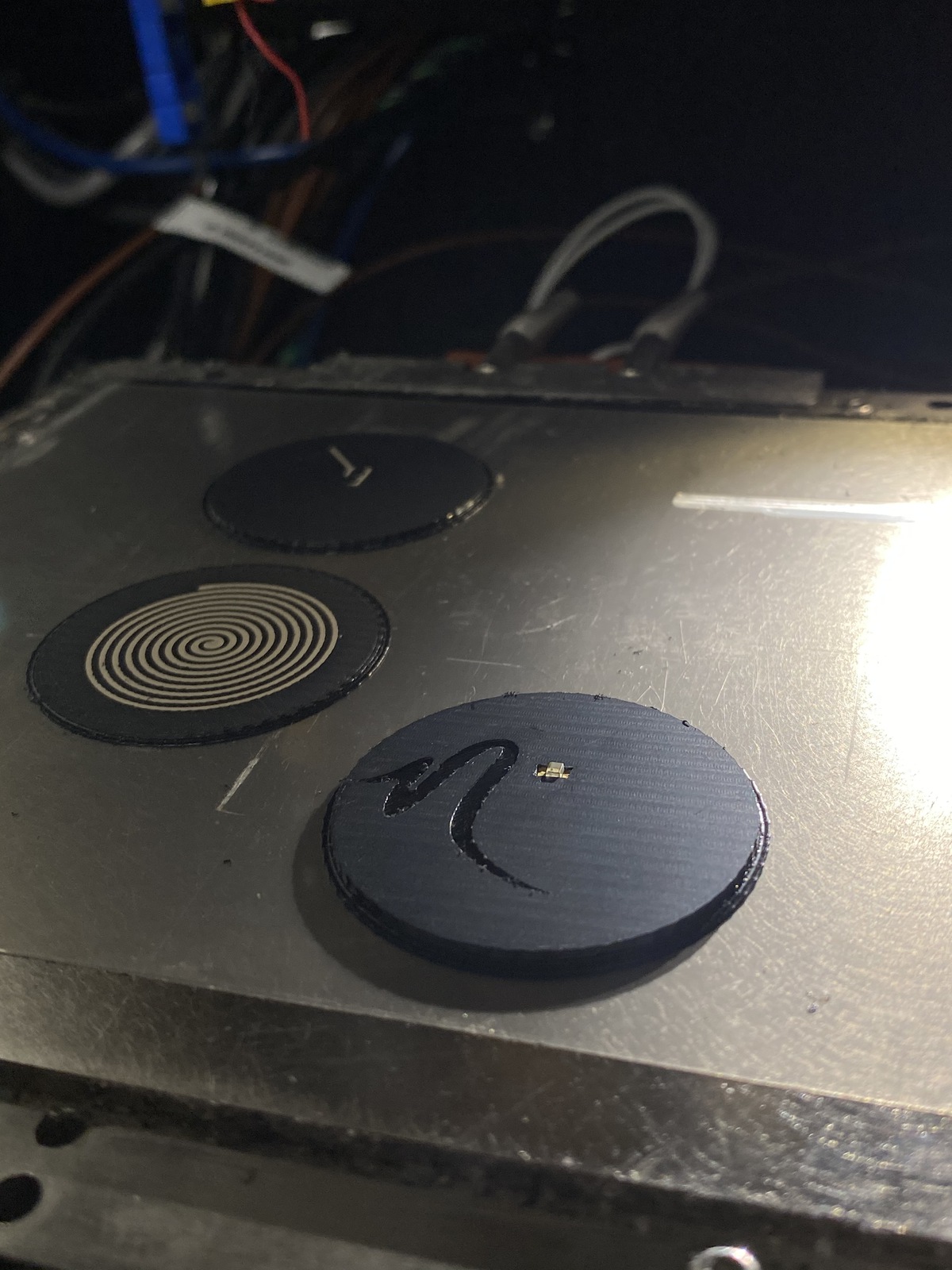
The discs were 3D manufactured using nScrypt’s Factory in a Tool (FiT). According to nScrypt’s CEO, Ken Church:
“We distinguish between printed circuit boards, which are incorporated into finished products, and printed circuit structures, or PCS, where the electronics and the structure or housing of a device are essentially the same thing.
“We’re doing a free live webinar about state of the art PCS on April 28 with rockstars in this area from Army, Air Force, NASA, SI2, University of Delaware, and DeLux Advanced Manufacturing.”
Anyone interested in the free webinar can register here.
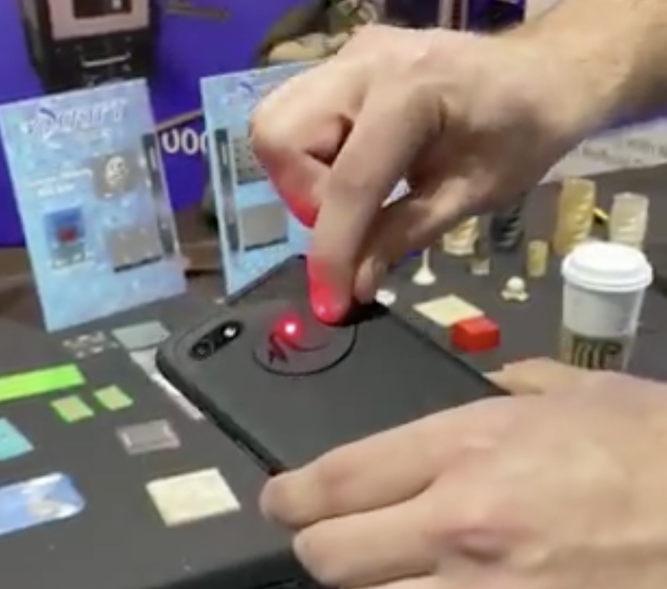
nScrypt also distinguishes between 3D printing, which is mostly making parts, and using its Factory in a Tool to 3D manufacture fully functioning finished products, like the inductor disc PCS. As shown in the video, nScrypt’s FiT first 3D prints the disc’s ABS outer shell using its material extrusion tool head (also known as FFF or FDM), then uses its SmartPumpTM tool head to microdispense conductive lines, then uses its material extrusion tool head to print another ABS layer, then uses its milling tool head to mill the intermediate layer smooth, then uses its pick and place tool head to place a Near Field Communication (NFC) chip and the SmartPump tool head to dispense more conductive paste, then completes the structure of the disc, seals in the electronics, and prints the nScrypt logo with the material extrusion tool head, then uses its milling tool head to provide a fine surface finish for the finished PCS.
Ken Church said:
“This is a cool little demonstration of a simple printed circuit structure with fine surface finish, where the electronics are embedded in the housing of the device with our Factory in a Tool. This disc happens to be flat but the FiT can 3D manufacture virtually any shape, conformally printing the electronics into or on device’s structure. The sky is the limit for 3D manufacturing PCS with our Factory in a Tool. Or maybe the sky isn’t the limit because a ruggedized version of our bioprinter, which has basically the same capability as our FiT, is on the International Space Station.”
The FiT system can be equipped with nVision cameras that monitor the tool heads for automated in-process inspection and computer vision routines, surface mapping for Z-tracking and conformal printing onto objects of any surface shape, UV LED curing light, and a HEPA filter.
The post nScrypt Demonstrates 3D Manufactured Printed Circuit Structure appeared first on 3DPrint.com | The Voice of 3D Printing / Additive Manufacturing.
3D Printing & Conductivity: Preparing New Polymer Bioinks for Electronics & Other Applications
International researchers delve into the area of materials science and 3D printing—a common theme today—but in this study, conductivity is the focus. Detailing their findings in the recently published ‘3D Printing of Conducting Polymers,’ the authors make it clear that while such polymers offer great potential in applications like electronics, there have still been challenges to overcome.
Upon developing a high-performance conducting polymer ink based on poly(3,4-ethylenedioxythiophene):polystyrene sulfonate (PEDOT:PSS), the researchers aimed to create a concentrated solution of nanofibrils.

a, b, Pristine PEDOT:PSS solution (a) can be converted into a 3D printable conducting polymer ink (b) by lyophilization in cryogenic condition and rdispersion with a solvent. c, 3D-printed conducting polymers can be converted into a pure PEDOT:PSS both in dry and hydrogel states by dry-annealing and subsequent swelling in wet environment, respectively. d CryoTEM image of a pristine PEDOT:PSS solution. e CryoTEM image of a 3D printable conducting polymer ink. f TEM image of a dry-annealed 3D-printed conducting polymer. g–j Images of re-dispersed suspensions with varying PEDOT:PSS nanofibril concentration. k SAXS characterization of conducting polymer inks with varying PEDOT:PSS nanofibril concentration. The d-spacing L is calculated by the Bragg expression L = 2π/qmax. l Apparent viscosity as a function of shear rate for conducting polymer inks of varying PEDOT:PSS nanofibril concentration. m Apparent viscosity of conducting polymer inks as a function of PEDOT:PSS nanofibril concentration. n Shear storage modulus as a function of shear stress for conducting polymer inks of varying PEDOT:PSS nanofibril concentration. o Shear yield stress of conducting polymer inks as a function of PEDOT:PSS nanofibril concentration. For TEM images in (d–f), the experiments were repeated (n = 5) based on independently prepared samples with reproducible results. Scale bars, 100 nm.
With ‘superior printability,’ the polymer ink offers a range of high-performance capabilities, printing with:
- High resolution
- High aspect ratio
- Overhanging structures
In this study, the researchers created print mesh samples of the ink via 200-, 100-, 50-, and 30-µm diameter nozzles. The structures could be easily transformed into dry or hydrogel form, with ‘long-term stability’ to be expected wet environments without degradation—even after storing for six months.
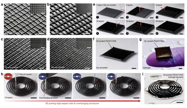
a–d SEM images of 3D-printed conducting polymer meshes by 200-µm (a), 100-µm (b), 50-µm (c), and 30-µm (d) nozzles. e Sequential snapshots for 3D printing of a 20-layered meshed structure by the conducting polymer ink. f 3D-printed conducting polymer mesh after dry-annealing. g 3D-printed conducting polymer mesh in hydrogel state. h Sequential snapshots for 3D printing of overhanging features over high aspect ratio structures by the conducting polymer ink. i 3D-printed conducting polymer structure with overhanging features in hydrogel state. Scale bars, 500 µm (a); 200 µm (b–d); 1 mm (a–d, inset panels); 2 mm (e–i).
The ink can also be integrated into multi-material 3D printing processes easily, proven during the study as the team created a structure similar to a high-density multi-electrode array (MEA) based on multi-material 3D printing of the conducting polymer ink and an insulating polydimethylsiloxane (PDMS) ink—all within 30 minutes.
“The 3D printed MEA-like structure shows a complex microscale electrode pattern and a PDMS well that are comparable to a commercially available MEA fabricated by multi-step lithographic processes and post-assembly,” stated the researchers.
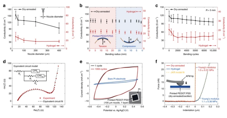
a Conductivity as a function of nozzle diameter for 3D-printed conducting polymers in dry and hydrogel states. b Conductivity as a function of bending radius for 3D-printed conducting polymers in dry (17 µm, thickness) and hydrogel (78 µm, thickness) states. PI indicates polyimide. c Conductivity as a function of bending cycles for 3D-printed conducting polymers in dry (17 µm, thickness) and hydrogel (78 µm, thickness) states. d Nyquist plot obtained from the EIS characterization for a 3D-printed conducting polymer on Pt substrate (78 µm, thickness) overlaid with the plot predicted from the corresponding equivalent circuit model38. In the equivalent circuit models, Re represents electronic resistance, Ri represents ionic resistance, Rc represents the total ohmic resistance of the cell assembly, CPEdl represents the double-layer constant phase element (CPE), whereas CPEg represents the geometric CPE. CPE is used to account inhomogeneous or imperfect capacitance and are represented by the parameters Q and n where Q represents the peudocapacitance value and n represents the deviation from ideal capacitive behavior. The true capacitance C can be calculated from these parameters by using the relationship C = Qωmaxn−1, where ωmax is the frequency at which the imaginary component reaches a maximum37. The fitted values for 3D-printed PEDOT:PSS are Re = 107.1 Ω, Ri = 105.5 Ω, Rc = 14.07 Ω, Qdl = 1.467 × 10⁻⁵ F sn−1, ndl = 0.924, Qg = 4.446 × 10⁻⁷ F sn−1, and ndl = 0.647. e CV characterization for a 3D-printed conducting polymer on Pt substrate. f Nanoindentation characterizations for 3D-printed conducting polymers in dry and hydrogel states with the JKR model fits. Values in (a–c) represent the mean and the standard deviation (n = 5 per each testing conditions based on independently prepared samples and performed experiments).
Because the polymers are highly reproducible, they can be 3D printed quickly with over 100 circuit patterns in less than 30 minutes, displaying ‘high electrical conductivity.’ This type of production offers an alternative to ink-jet or screen printing—along with greater versatility in design options, depending on required applications.
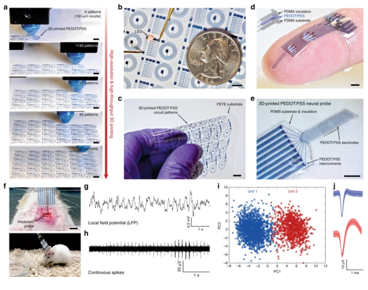
a Sequential snapshots for 3D printing of high-density flexible electronic circuit patterns by the conducting polymer ink. b Lighting up of LED on the 3D-printed conducting polymer circuit. PETE indicates polyethylene terephthalate. c Bending of the 3D-printed conducting polymer circuit without failure. d Image of the 3D-printed soft neural probe with 9-channels by the conducting polymer ink and the PDMS ink. e Image of the 3D-printed soft neural probe in magnified view. f Images of the implanted 3D-printed soft neural probe (top) and a freely moving mouse with the implanted probe (bottom). g, h Representative electrophysiological recordings in the mouse dHPC by the 3D-printed soft neural probe. Local field potential (LFP) traces (0.5 to 250 Hz) under freely moving conditions (g). Continuous extracellular action potential (AP) traces (300 to 40 kHz) recorded under freely moving conditions (h). i Principal component analysis of the recorded single-unit potentials from (h). j Average two units spike waveforms recorded over time corresponding to clusters in (i). Scale bars, 5 mm (a–c); 1 mm (d, e); 2 mm (f).
Experiments were performed using a customized Cartesian gantry style 3D printer by Aerotech, offering a variety of nozzle sizes. Conductivity was measured in the 3D printed polymers as the researchers employed a four-point probe. Samples were prepared via one layer of conducting polymer ink printed into a rectangular shape of 30 mm in length and 5 mm in width, featuring 100-µm nozzles on glass substrates, and copper wire electrodes attached with silver paste to the surfaces.
“This work not only addresses the existing challenges in 3D printing of conducting polymers but also offers a promising fabrication strategy for flexible electronics, wearable devices, and bioelectronics based on conducting polymers,” concluded the researchers.
3D printing and electronics accompany each other—whether in the form of newly developed composites for greater functionality, in use with smart textiles, circuit boards, or other useful technologies. Experiments and innovations regarding 3D printing and conductive materials are becoming increasingly popular too as users, researchers, and manufacturers look for better ways to create more powerful parts.
What do you think of this news? Let us know your thoughts! Join the discussion of this and other 3D printing topics at 3DPrintBoard.com.
[Source / Images: ‘3D Printing of Conducting Polymers’]
The post 3D Printing & Conductivity: Preparing New Polymer Bioinks for Electronics & Other Applications appeared first on 3DPrint.com | The Voice of 3D Printing / Additive Manufacturing.
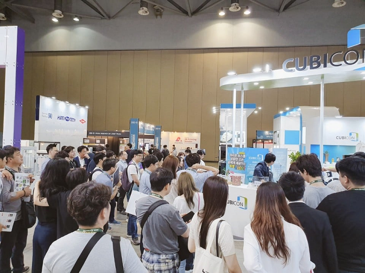
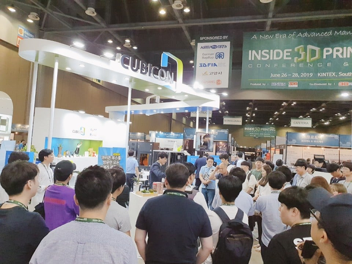
South Korea’s Largest 3D Printing Event Takes Place on June 24-26 as Planned
Inside 3D Printing Seoul is entering its 7th year and has become one of Asia’s premier additive technology events for digital transformation of design, development and manufacturing driven by Industry 4.0.
With 20% year-on-year growth in exhibitor numbers and 25% annual growth in floor space sold, Inside 3D Printing Seoul has positioned itself as the powerhouse for industrial additive manufacturing in Asia.
“We have participated in dozens of exhibitions both in Korea and abroad. Now we found that Inside 3D Printing Seoul is the best marketing platform for our industry-level 3D printers in manufacturing, dental and jewelry field.” commented Yong-ho Choi, General Manager of Hepzibah.
“According to my partner in Korea, Inside 3D Printing Seoul has become South Korea’s largest and best market place since 2014.” said Liam Marriott, APAC Channel Marketing Manager of Formlabs. He also added, “This year, we are to exhibit our brand new products and services with largest scale, ever.”
“If we have to choose one event out of dozens of other 3D technology events in APAC region, that would be Inside 3D Printing Seoul because this is the only one with brand, contents and quality buyers.” mentioned Yoon-Jae Lee, Marketing Manager of Hanil Protech. “That is why we are participating as a Silver Sponsor for 5 consecutive years in a row.”
Unlike a number of non-specialized events in Asia, Inside 3D Printing Seoul brings the 9,000+ active industrial AM users as well as supplier groups together every year. This event is the best launch pad for both domestic companies looking for a global audience and for international companies looking to tap the Korean market.
In addition to increasingly popular composite materials, specific special materials will also be refined and simplified, which will be put into large-scale application. Moreover, 3D metal printing is rising rapidly in Asia and will play a crucial role in major industries including automobile, aerospace, health care and consumer electronics in the near future.
Inside 3D Printing Seoul boasts its 30+ world-class speakers with practical application cases in 4 tracks; Metal, Manufacturing, Aerospace/Automotive and Medical/Dental.
Dozens of industry professionals are already confirmed as major speakers including: Benoit Valin, General Manager, Essentium; Alan Yu, Application Engineering Manager, Markforged; Byoungjik Lim, Senior Researcher, Korea Aerospace Research Institute or KARI; Simon Lee, Regional Director, AM Ventures GmbH; Sang Joon Park, Founder and CEO, MEDICAL IP.
Further enhancing this year’s event, 3DPrint.com and SmarTech Analysis join as co-producers, further upgrading the event and providing the best marketing platform for 90+ exhibitors, sponsors and 9,000+ buyers from around the world.
Limited availability still remains to speak and/or exhibit before 9,000+ buyers and influencers around the globe until April 30, 2020 with increased discount rate.
If interested in exhibiting or speaking opportunities for this forthcoming Seoul event taking place on June 24-26, please contact Inside 3D Printing Secretariat (inside3dprinting@kintex.com) or visit our website (www.inside3dprinting.com/seoul) for more information.
The post South Korea’s Largest 3D Printing Event Takes Place on June 24-26 as Planned appeared first on 3DPrint.com | The Voice of 3D Printing / Additive Manufacturing.
Eight industrial partners set to work on modular hybrid manufacturing system
A joint research project funded by the German Federal Ministry for Education and Research (BMBF) will see the development of a new highly efficient modular hybrid manufacturing cell. The eight-partner ProLMD project was initiated four years ago, with the initial aim of producing new hybrid manufacturing processes that combine conventional methods with the laser material […]
UK researchers create low-cost electrospray and electrospinning device using FDM 3D printing
Researchers from the University of Edinburgh have used FDM 3D printing to fabricate a low-cost electrospray/electrospinning device intended for biomedical applications. Although leveraging different techniques, both electrospray and electrospinning methods use analogous technology for the production of nanostructures. Electrospinning enables the production of polycaprolactone fibers with diameters in the order of some hundred nanometers. Electrospray ionization […]